
 日本語
日本語
 한국어
한국어

A Complete Guide to Flying Probe Testing in PCB Manufacturing
KEY DEFINITION Flying probe testing is an automated electrical test method that verifies PCB quality using movable probes driven by CAD data, without requiring a custom fixture. It detects shorts, opens, resistance, capacitance, and component placement errors, making it the dominant test strategy for prototypes, low-to-medium volume production, and high-density interconnect (HDI) boards where traditional bed-of-nails ICT is too slow to set up or too expensive to justify.
What Is Flying Probe Testing?
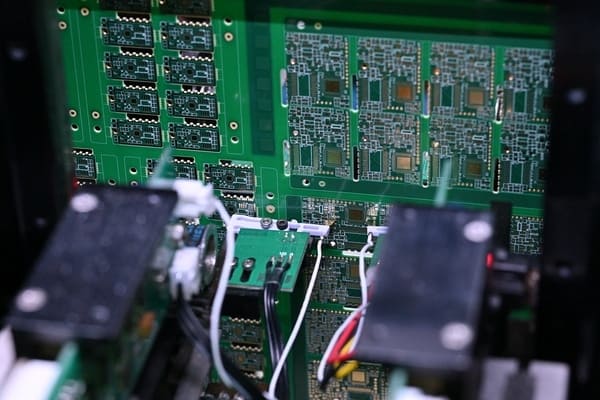
A flying probe test (FPT) uses one or more precision probes mounted on high-speed X-Y gantries that "fly" across the surface of a PCB, landing on individual test points in sequence to perform electrical measurements. The probe movement paths, test point coordinates, and measurement parameters are all generated directly from the board's CAD data, Gerber files, and netlist, not from a physical fixture.
This is the fundamental difference from In-Circuit Testing (ICT). ICT uses a custom-machined "bed of nails" fixture with spring-loaded pogo pins arranged in a fixed pattern that matches one specific board design. Every time the board design changes, the fixture must be redesigned and remanufactured. Flying probe testing eliminates this dependency entirely. A design change means updating a software file, not machining a new $20,000 block of metal.
The technology emerged in the late 1980s, driven by the increasing density of surface-mount designs and the shortening of product development cycles. Traditional ICT fixtures were taking weeks to fabricate at a time when engineering teams needed test results in hours. Flying probe testers filled that gap and have since become standard equipment in virtually every PCB prototype and quick-turn fabrication shop.
How the Test Actually Runs
The process follows four stages, and understanding each one matters because it determines what defects the test catches and what it misses:
1. Test program generation from CAD data. The test engineer imports the board's Gerber files, drill files, netlist, and bill of materials (BOM) into the flying probe test software. The software extracts all node coordinates, assigns test point priorities, and generates optimized probe movement paths to minimize total test time. This is the step that replaces fixture design in the ICT world, and it typically takes 30 minutes to a few hours depending on board complexity and node count.
2. Board loading and optical alignment. The bare board or assembled PCB is placed on the test platform. High-resolution cameras locate fiducial markers on the board surface to establish a precise coordinate reference. This optical registration corrects for any minor mechanical misalignment in board placement and ensures the probes land on their intended targets within micron-level accuracy, even on boards with 0.4 mm pitch BGAs or 0201 passive components.
3. Sequential probe movement and measurement. The probes move from test point to test point in the programmed sequence. At each landing site, the probe tip makes physical contact with the copper pad or component lead, and the tester performs the specified measurement: continuity (shorts and opens), resistance (2-wire or 4-wire Kelvin measurement for values below 1 ohm), capacitance, inductance, diode polarity, and for assembled boards, passive component values against the BOM tolerance. On a typical 500-node board, this takes 2 to 8 minutes. On a 5,000-node complex board, it can take 20 to 30 minutes.
4. Fault reporting and diagnostics. A pass/fail verdict is generated for each test point. Crucially, the tester identifies not just that a failure occurred but precisely which node is at fault and what measurement value was recorded versus what was expected. This node-level diagnostic resolution is one of the strongest arguments for flying probe testing in debug-intensive environments like new product introduction (NPI) and engineering validation.
Flying Probe Test vs. In-Circuit Test: The Comparison That Drives Your Decision
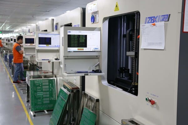
This is the question every PCB project manager eventually faces. Here is the direct comparison, with real numbers, because aggregate generalities will not help you choose.
| Dimension | Flying Probe Test (FPT) | In-Circuit Test (ICT) |
|---|---|---|
| Fixture cost | $0 (no fixture required) | $8,000 to $25,000 per fixture |
| Fixture lead time | None (CAD-driven) | 3 to 6 weeks |
| Test speed | 1 to 30 minutes per board | 5 to 120 seconds per board |
| Design change flexibility | High (update software file only) | Low (new fixture required) |
| Per-board cost at volume | Higher (serial testing) | Lower (parallel, amortized fixture) |
| Min test point pitch | 0.2 mm (8 mil) typical | 0.5 mm (20 mil) typical |
| Hidden joints (BGA, QFN pad) | Not testable | Not testable |
The Volume Crossover Point
The economic crossover between FPT and ICT depends on board complexity, production volume, and fixture amortization. A widely cited industry heuristic places the break-even at roughly 1,000 to 2,000 boards per design revision. Below that volume, the fixture cost of ICT dominates the per-board economics. Above that volume, the faster test speed of ICT pays back the fixture investment.
However, this heuristic is shifting. Modern flying probe testers from manufacturers like Seica, Takaya, and SPEA now use four or eight simultaneously moving probes, doubling or quadrupling test throughput compared to single-probe architectures. Some high-end systems now test a 1,000-node board in under 3 minutes, making the crossover point with basic ICT increasingly contestable well into the mid-volume range.
Why Many Shops Run Both
In practice, many medium-to-high volume PCB assembly lines use a layered test strategy. Flying probe testing validates prototypes, and first-article builds at NPI. ICT takes over for volume production once the design is stable. Automated Optical Inspection (AOI) runs in parallel on the SMT line for visible defects. Functional test (FCT) validates end-to-end system behavior at the final stage. No single test method covers everything, and flying probe testing occupies the critical bridge between design validation and production ramp.
When to Choose Flying Probe Testing: The Five Application Scenarios
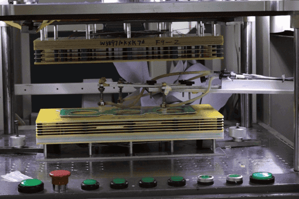
There are specific situations where flying probe testing is not just an option but the clearly correct choice. Here they are, ranked from most common to most specialized.
Prototype and engineering validation builds. When you build five or ten boards to validate a new design, spending $15,000 on an ICT fixture that will be obsolete by the next board spin is economically irrational. Flying probe testing gives you comprehensive electrical validation on those first boards with zero tooling cost and setup that completes in hours, not weeks.
Low to medium volume production, especially with frequent design revisions. In industries like medical devices, aerospace, and industrial controls, production runs of 50 to 500 units are common, and regulatory or performance changes may trigger board revisions every six months. Flying probe testing absorbs these changes at zero incremental cost while delivering consistent test coverage across every revision.
High-density interconnect (HDI) PCBs with fine-pitch components. When a board uses 0.4 mm pitch BGAs, 0201 passives, or micro-via-in-pad structures, the physical density exceeds what a bed-of-nails fixture can reliably contact. A flying probe's single fine-point tip can reach individual test pads within these dense geometries without the mechanical alignment challenges that plague multi-pin fixtures at sub-0.5 mm pitch.
Boards with limited test point access on one side. Some designs restrict test pad placement to a single side due to component density, shielding requirements, or connector placement. Flying probe testers with dual-side probing capability can access both top and bottom surfaces simultaneously, a flexibility that ICT fixtures struggle to match without complex and expensive dual-stage mechanical designs.
Quick-turn fabrication where turnaround time dominates cost sensitivity. When a customer needs boards tested and shipped within 24 to 48 hours, the three-to-six-week lead time for an ICT fixture is simply not on the table. Flying probe testing is the only electrical test method that can deliver comprehensive validation on a quick-turn schedule. PCBgogo, for instance, integrates flying probe testing as a standard quality gate in its quick-turn PCB fabrication flow, running test programs generated directly from the customer's submitted Gerber files without adding fixture lead time to the order.
Limitations: What Flying Probe Testing Cannot Do, and What You Need Instead
No test method is universal. Understanding where flying probe testing fails is more important than knowing where it succeeds, because the failures happen at the worst possible time: after you have already committed to the method.
Hidden solder joints are invisible. Any joint that a probe tip cannot physically reach (BGA balls, QFN thermal pads, connectors with shrouded contacts, chip-scale packages with balls on the underside) cannot be tested by flying probe. The only complementary methods are X-ray inspection (2D or 3D/CT for BGA void detection and solder joint morphology) and functional test (verifying the system actually works end to end).
Test speed does not scale with volume. Because flying probe testing is inherently serial (one probe lands on one test point at a time), the total test time grows roughly linearly with the number of test nodes. On a 5,000-node board, 20 to 30 minutes per board is realistic. At 500 boards, that adds up to more than 200 hours of tester time. ICT, by contrast, tests all nodes in parallel and completes the same board in under two minutes regardless of node count. The cost crossover is a mathematical certainty, not an opinion.
High-frequency signal integrity is not verified. Flying probe testing measures DC and low-frequency parameters: continuity, resistance, capacitance, inductance. It does not generate eye diagrams, does not measure insertion loss (S21), and does not verify impedance control at frequency. For boards carrying PCIe, USB 3.0, DDR memory buses, or RF signals above 100 MHz, separate testing (TDR impedance testing on coupons, vector network analyzer measurements, or dedicated high-speed functional test) is mandatory.
Probe tips can leave cosmetic marks. The physical contact between probe tip and test pad leaves a small dimple, typically 25 to 50 microns in diameter. For most applications this is cosmetic and functionally irrelevant. However, on gold-plated contacts for edge connectors or on critical RF pads where surface roughness affects impedance, even this small mark may be objectionable. Discuss probe landing site selection with your fabricator if specific pads are visually or electrically sensitive.
Test coverage is only as good as the test point strategy. Flying probe testing can only measure what it can reach. If the designer did not include dedicated test points for critical nets (routing them only between component pads with no exposed copper for probing), those nets go electrically unverified. This is a design-for-test (DFT) issue, not a limitation of the test equipment itself, but it is the single most common reason flying probe test coverage falls below 90%. Every critical net needs an exposed, unmasked test pad accessible from at least one side of the board.
The Flying Probe Testing Process from Design to Report: A Step-by-Step Walkthrough
For engineers who need to integrate flying probe testing into their production flow, here is the end-to-end process with enough detail to actually act on.
Step 1: Prepare DFT-compliant design files. Before submitting a board for flying probe testing, verify that all critical nets have accessible test points. A test point is simply an exposed copper pad (no solder mask) on an outer layer, at least 0.5 mm in diameter and spaced at least 0.5 mm from adjacent pads. Include test points for power nets, ground nets, and every net that carries a critical signal. Avoid placing test points under tall components or inside connectors where probe reach is mechanically blocked. Export Gerber files, the Excellon drill file, the IPC netlist (IPC-D-356 format is preferred), and the bill of materials if assembled boards are being tested.
Step 2: Test program generation. Import the design files into the flying probe tester's programming environment. The software extracts all net nodes, assigns test point coordinates, and generates an optimized probe movement sequence. For assembled boards, the BOM is cross-referenced to assign expected component values to each part location. Most modern testers can also import CAD data in ODB++ or IPC-2581 format, which preserves netlist and component data in a single file and reduces programming errors caused by file format mismatches.
Step 3: First-article debug and optimization. Run the test program on the first board. Expect the first run to produce false failures. This is normal. Misaligned fiducial recognition, probe landing on a via tented with non-conductive residue, or a component tombstone that blocks probe access all produce failures that are real physical obstacles to measurement but not actual electrical defects. The test engineer adjusts the program iteratively until the first-article board passes cleanly or reveals genuine electrical faults. This debug cycle typically adds 30 to 90 minutes to the first board and is a one-time cost per design revision.
Step 4: Production testing and reporting. Once the program is validated, subsequent boards run unattended. The tester generates a pass/fail report for each board, typically archived by serial number or batch ID for traceability. In regulated industries (medical, aerospace, automotive), these test reports are part of the device history record and must be retained for the product's audit lifetime. Flying probe test data, because it is natively digital, integrates directly into manufacturing execution systems (MES) without the paper-to-digital translation step that older ICT systems sometimes require.
How Much Does Flying Probe Testing Cost?
Pricing on flying probe testing is rarely broken out, since it's usually bundled into the fabrication or assembly quote. Here's the real breakdown.
Bare board testing typically adds 5–15% to fabrication cost. A simple 2-layer board (~200 nets) might add $1–3 per board; a complex 12-layer HDI board (~3,000 nets) might add $15–30. More nets means more probe movements, and tester time is the real cost driver.
Assembled board testing adds more, typically 15–30%, since the test program also checks component values, placement, and polarity, taking longer per board.
Test fixtures are a separate, one-time cost, not a per-board fee. A fixture for ~1,000 test points runs about $55. Customers can supply their own or have the fabricator source one, whichever is easier.
At PCBgogo, both methods run in-house on our own equipment. Small-batch and prototype orders default to flying probe for fast turnaround with no tooling wait; production-volume orders shift to test fixture testing for higher per-board test speed. That means test capacity scales with order size instead of becoming a bottleneck, and delivery timelines hold up whether you're ordering 5 boards or 5,000.
Frequently Asked Questions
What is the difference between flying probe testing and ICT?
Flying probe testing uses movable probes driven by CAD data and requires no custom fixture. ICT uses a fixed bed-of-nails fixture specific to one board design. Flying probe is faster to set up and cheaper for low volumes but slower per board. ICT is more expensive to set up but faster per board and becomes cost-effective above roughly 1,000 to 2,000 units per design revision.
How long does a flying probe test take?
For a typical board with 300 to 800 test nodes, expect 2 to 8 minutes. A complex board with 3,000 to 5,000 nodes can take 20 to 30 minutes. Simple 2-layer boards with fewer than 200 nodes may complete in under 90 seconds. Test time scales approximately linearly with node count, which is why volume economics eventually favor parallel ICT.
Can flying probe testing detect all PCB defects?
No. Flying probe testing detects electrical defects: shorts, opens, incorrect resistance or capacitance, missing or wrong-value components, and diode polarity errors. It does not detect visual defects (solder bridging visible only from the side, insufficient solder wetting, tombstoning that does not create an open circuit), internal structural defects (BGA voiding, inner-layer delamination), or high-frequency signal integrity issues. A complete quality strategy combines flying probe testing with AOI, X-ray inspection, and functional test.
Is flying probe testing suitable for mass production?
Generally no, unless production volumes are under 1,000 units per design revision or the board density makes ICT fixturing impractical. At high volumes, the per-board test time of flying probe becomes the bottleneck, and ICT's upfront fixture cost is amortized across the production run to deliver a lower per-board test cost.
Do flying probe tests leave marks on the PCB?
Yes. The probe tip leaves a small dimple, typically 25 to 50 microns in diameter, at each contact point. On standard copper pads, this is invisible to the naked eye and electrically irrelevant. On gold-plated edge connector pads or critical RF traces, specify alternative test point locations or accept a small cosmetic mark. Most fabricators will avoid probing visually or electrically sensitive pads if you note them in the fabrication drawing.
What files do I need to provide for flying probe testing?
At minimum: Gerber files (all copper and solder mask layers), the Excellon drill file, and the IPC netlist (IPC-D-356 format preferred). For assembled board testing, also include the bill of materials (BOM) and component placement file (pick-and-place / centroid data). ODB++ and IPC-2581 formats combine all of these into a single file and reduce the risk of version mismatches between separate design outputs.
Conclusion
Flying probe testing works best as one layer in a broader QA strategy, alongside AOI, X-ray, and functional test. PCBgogo runs flying probe testing across both prototype and volume PCB/PCBA orders, with test programs generated directly from your submitted Gerber files for fast turnaround. Get your instant quote and start your build.





