Why PCB Tooling Strips Are Vital in SMT Assembly?
You might notice extra strips of "waste" material on the sides of a PCB panel during PCBA processing. These are known as PCB Tooling Strips (or Process Edges). While they are eventually removed and discarded, they are far from useless.
For electronics designers and manufacturers, understanding the role of these edges is the difference between a smooth production run and a high-defect nightmare. As a professional PCBA manufacturer, we’re pulling back the curtain on why these 5–10mm strips are essential for quality and efficiency.

What Exactly is a PCB Tooling Strip?
A tooling strip is a designated area on the edge of a PCB that contains no electronic components or functional circuitry. Usually measuring between 5mm and 10mm in width, these strips are added to the panel design specifically to facilitate the SMT (Surface Mount Technology) and DIP (Dual In-line Package) assembly processes. Once the components are soldered and the board is tested, these edges are removed via V-scoring or "mouse bite" tabs.
5 Critical Functions of Process Edges
1. Providing Vital Clamping Space
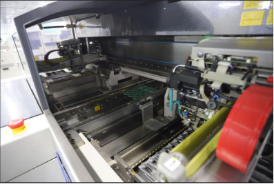
Automation is the heart of modern SMT lines. As your PCB moves through pick-and-place machines, reflow ovens, and wave soldering equipment, it travels on conveyor belts. These machines use mechanical clamps to hold the board in place.
Tooling strips provide the necessary "grip" area for these clamps. Without them, the machines would have to grip the functional area of your board, potentially crushing components or interfering with the placement of parts near the edge.
2. Facilitating High-Speed Machine Operations
Modern SMT machines operate at incredible speeds. To maintain accuracy, they need clear "safe zones" for positioning. Tooling strips often house Fiducial Marks—small copper circles that act as optical reference points for the machine's cameras. Having these markers on the process edge ensures the machine can calibrate its position without taking up valuable real estate on your functional circuit.
3. Protecting Edge Components from Mechanical Stress
Components placed too close to the board edge are vulnerable. During handling, transport, or the final "de-panelization" process (cutting the boards apart), the edges of the PCB undergo significant mechanical stress. Tooling strips act as a sacrificial buffer, absorbing this stress and preventing micro-cracks in ceramic capacitors or solder joints near the perimeter.
4. Streamlining Testing and AOI
After assembly, boards undergo AOI (Automated Optical Inspection) and sometimes X-ray or ICT (In-Circuit Testing). Tooling strips allow these inspection machines to secure the board firmly without obstructing the view of the components. In some advanced designs, the strips even hold temporary test points used for initial power-on trials before the board is finalized.
5. Improving Soldering Consistency
Whether it's reflow or wave soldering, thermal management is key. Tooling strips help balance the thermal mass of the board. In wave soldering, specifically, they prevent the "shadow effect" and help manage the flow of the molten solder, ensuring that the pins on the edge of the board receive a clean, reliable fillet rather than a bridge or a cold joint.
Why Skipping PCB Tooling Strips Costs You More
It might be tempting to eliminate process edges to save on raw material costs, but this is a classic case of "penny wise, pound foolish." Here is how a lack of tooling strips impacts your bottom line:
Precision Issues: Without a stable clamping area, the board can vibrate or shift slightly during pick-and-place, leading to offset components and manual rework.
Physical Damage: The risk of "pop-off" components or cracked traces increases by over 40% when components are placed directly against the conveyor contact zone.
Reduced Throughput: Technicians often have to slow down the machines or perform manual "workarounds" to handle boards without edges, significantly extending your production lead time.
The Verdict: Small Detail, Big Impact
While they seem like an afterthought, PCB tooling strips are the "scaffolding" that allows your PCB to be built with precision. They ensure your components stay safe, your solder joints stay strong, and your production costs stay predictable.
At PCBGOGO, we specialize in high-precision PCBA assembly. We don't just build boards; we optimize them. Our engineering team provides a free DFM (Design for Manufacturability) review for every order, ensuring your tooling strips and panel layouts are perfectly configured for the highest possible yield and reliability. Contact us freely!

