Why PCB Laser Depaneling is Superior to Traditional Methods?
In the SMT (Surface Mount Technology) assembly workflow, depaneling is one of the final and most critical stages. To maximize production efficiency, many designs utilize a "panelized" layout—combining multiple small boards into a single large panel for processing. Once assembly is complete, these boards must be separated into individual units.
While traditional mechanical methods have been the standard for years, PCB Laser Depaneling has emerged as a specialized technology that offers significant advantages. Compared to traditional milling or manual cutting, its strengths lie in high precision, zero mechanical stress, and clean edges, making it the ideal choice for high-density and high-precision circuit boards.

The Pain Points of Traditional Depaneling
To understand why PCB Laser Depaneling is becoming the industry standard for high-end electronics, we must first look at the limitations of conventional methods:
Manual Cutting: This involves hand-operated tools like shears. It is inefficient and frequently causes edge cracking or component displacement. Because the precision is extremely poor, it is only suitable for low-end boards with loose tolerances.
Milling Cutter Depaneling: This is a common mechanical method using a high-speed rotating bit.5 However, it presents two major risks. First, the physical contact generates mechanical stress. This stress travels through the board to the solder joints of sensitive components like BGA or QFN chips, causing latent micro-cracks. Second, the cutting accuracy is limited; for tightly packed panels, the bit can easily drift and damage the effective circuit area.
The Advantages of PCB Laser Depaneling
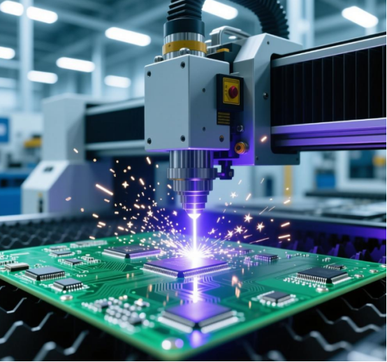
The PCB Laser Depaneling process operates on a completely different principle. As a non-contact technology, it uses a high-energy laser beam to burn and melt the connecting tabs along a pre-programmed path. Here are the three core dimensions where this process excels:
1. Extreme Cutting Precision
A laser beam’s spot diameter can be controlled to under 0.01mm, achieving path accuracy within ±0.02mm—a level of detail far beyond the reach of a mechanical mill. For high-density boards used in smartphones or IoT modules, where the spacing between boards may be as narrow as 0.5mm, the laser can navigate the gap perfectly without damaging neighboring traces or components.
2. Zero Mechanical Stress
Because PCB Laser Depaneling is non-contact, no physical force is applied to the board. This eliminates the risk of "hidden" solder joint fractures. This is vital for mission-critical electronics in the automotive and medical sectors, where high reliability is non-negotiable and a single latent defect could lead to catastrophic failure.
3. Smooth Edges without Burrs
Laser-cut edges are exceptionally smooth and free of burrs or frayed fiberglass.8 Traditional milling often leaves behind debris or rough edges that require manual sanding—a step that adds cost and risks introducing conductive dust into the assembly, which could cause short circuits. PCB Laser Depaneling provides a "finished" edge immediately after the cut.
Balancing Quality and Cost
It is worth noting that PCB Laser Depaneling generally carries a higher operational cost and slower throughput than mechanical milling. However, for boards requiring high precision and long-term reliability, the investment is well-justified.
In summary, the core strengths of PCB Laser Depaneling—high precision, low stress, and superior edge quality—make it the essential specialized SMT technique for solving the challenges of modern, high-density electronic manufacturing. To ensure your high-precision boards are handled with the best equipment and expertise, consider the advanced manufacturing solutions offered by PCBGOGO.

