
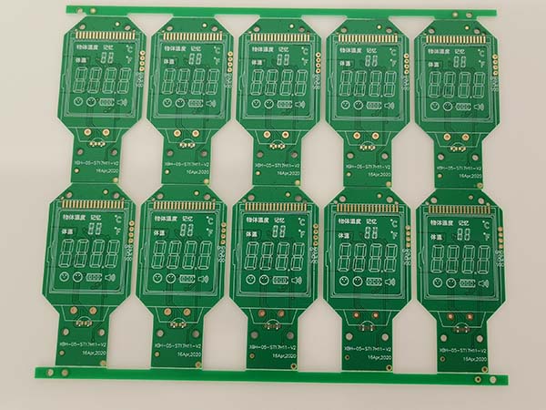
Why Is PCB Panelization Essential for Modern SMT Assembly Efficiency?
In high-volume electronics manufacturing, efficiency and cost reduction are paramount. The process of assembling surface mount technology (SMT) components onto a Printed Circuit Board (PCB) often requires a strategic preparation step known as PCB Panelization. This technique involves arranging multiple identical (or sometimes different) smaller PCBs onto a single, larger array, or panel, for simultaneous processing. The panelization process is not merely a convenience; it is a critical engineering decision that fundamentally impacts throughput, quality, and the overall cost effectiveness of the PCBA production cycle.
The Strategic Advantages of PCB Panelization
Panelization is required because most small or irregularly shaped PCBs cannot be handled reliably by automated SMT machinery (such as screen printers, pick-and-place machines, and reflow ovens) as individual units. Grouping them into a single, standardized panel size unlocks several key operational and financial benefits:
Optimized Production Throughput:
Reduced Cycle Time: Printing solder paste, placing components, and running through the reflow oven is done once for the entire panel, rather than multiple times for individual boards. This dramatically boosts the overall speed and capacity of the SMT line.
Machine Efficiency: By processing a single, larger unit, the setup and indexing time of the equipment is minimized, maximizing the time the machine is actively placing components.
Cost and Material Savings:
Material Utilization: Panelization allows for a better nesting and arrangement of individual PCBs, minimizing the wasted space (or "scrap area") on the larger raw PCB laminate, thereby improving material utilization.
Logistics and Handling: Large, standardized panels are easier and less costly to store, package, and ship compared to managing numerous small, loose units.
Enhanced Process Control:
Stability and Alignment: Small, thin boards are prone to warping (bow and twist) during high-temperature reflow soldering. Mounting them in a larger, rigid panel improves stability and ensures accurate component placement and solder joint consistency.
Fewer Defects: Consistency in the assembly process, facilitated by stable panels, naturally leads to a reduction in manufacturing defects.
Common Panelization Methods
The method chosen for PCB Panelization depends heavily on the board's shape, component placement (especially near the edges), and the required separation method after assembly (depanelization).
V-Scoring (V-Cut Panelization):
Application: Ideal for boards with regular, linear edges and no components positioned close to the edge.
Method: A V-shaped groove is cut approximately one-third of the way through the board from both the top and bottom sides. The finished boards are later separated by specialized depaneling tools or by snapping them along the score lines.
Tab Routing with Breakaway Tabs (Mouse Bites):
Application: Essential for irregular-shaped PCBs or boards with components placed right up to the edge.
Method: The individual boards are connected by narrow tabs containing a series of small, perforated holes (mouse bites). This allows the boards to remain connected during assembly but easily separated later without damaging sensitive components.
Slot Routing and Combined Methods:
This is often used for highly irregular shapes or when extra rigidity is needed, involving routing slots and using specialized tabs to secure the array. The final depanelization must be performed carefully to avoid inducing stress on the components.
Conclusion
Effective PCB Panelization is a fundamental cornerstone of a successful manufacturing strategy, directly impacting the throughput and financial viability of high-volume electronic assembly. It transforms challenging, small, or irregular boards into stable, machine-ready arrays, optimizing every stage from solder paste printing to reflow soldering. For partners requiring expert design-for-manufacturability (DFM) analysis and highly optimized production, PCBGOGO provides industry-leading PCBA services. Our capabilities in SMT manufacturing include advanced, flexible PCB Panelization techniques to accommodate any board geometry, ensuring maximum efficiency, quality, and fast turnaround for your projects. Contact us freely!

