
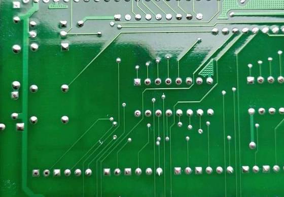
Why Does Solder Spiking Occur in PCBA Processing and How to Prevent It?
In the specialized field of Printed Circuit Board Assembly (PCBA), achieving flawless solder joints is critical for product longevity and performance. One common and problematic defect, particularly prevalent in wave soldering processes, is Solder Spiking, also known as "solder icicles" or "peaks." This defect manifests as a sharp point or peak of solder protruding from the solder joint, compromising the aesthetic quality and potentially the integrity of the board. Understanding the root causes of Solder Spiking is the first step toward high-reliability manufacturing.
Key Factors Contributing to Solder Spiking
The formation of Solder Spiking is fundamentally related to the poor separation of molten solder from the PCB surface as it exits the wave. This inability to cleanly detach is influenced by a combination of material science, process parameters, and design factors.
1. Solder Wettability and Flux Issues
Description: Poor wetting behavior of the molten solder.
Causes:
Insufficient or Low-Activity Flux: If the flux content is inadequate or its activity has decreased (e.g., due to excessive preheating), it fails to clean the metallic surfaces effectively, hindering the smooth flow and retraction of the solder.
Oxidized Surfaces: Contaminants, dirt, or excess oxides on the PCB pads or component leads interfere with the surface tension dynamics necessary for a clean break from the solder wave.
Proactive Strategy: Ensure the correct flux application amount and verify the flux activity level. Maintain a clean PCB surface prior to the wave soldering process.
2. Wave Soldering Temperature Deviations
Description: Incorrect settings for preheating or the main solder pot temperature.
Causes:
Excessively Low Temperature: A low solder pot temperature causes the solder's fluidity to decrease excessively upon contact with the PCB. The viscous solder clings to the joints, resulting in residual peaks.
Excessively High Temperature: Overheating can cause the flux to completely burn off (coke) prematurely, reducing its cleaning and protective action. The impaired wettability leads to poor solder flow and subsequent peaking.
Proactive Strategy: Calibrate the temperature sensors regularly. Establish and strictly adhere to an optimized thermal profile that ensures the PCB reaches the necessary activation temperature without prematurely destroying the flux.
3. PCB Design and Fabrication Quality
Description: Defects originating from the PCB substrate itself influence the solder's adherence.
Causes:
Uneven Copper Foil/Surface Finish: Issues during the PCB manufacturing, such as incomplete or over-etching, can create an uneven surface topography on the pads, disturbing the smooth flow of the molten solder.
Proactive Strategy: Implement rigorous Incoming Quality Control (IQC) for bare PCBs, including surface inspection and dimensional checks. Adhere to Design for Manufacturability (DFM) guidelines, which specify proper pad geometry and spacing.
4. Process Speed and Immersion Depth
Description: How the PCB interacts mechanically with the molten solder wave.
Causes:
Excessively Long Contact Time: A slow conveyor speed leads to an extended contact time, which can overheat the joint area, prolonging the solidification time and promoting the formation of peaks as the board exits the wave.
Excessive Immersion Depth: If the board is dipped too deeply, the solder contact angle is altered, and a large volume of solder is adhered. The separation point becomes unstable, causing the solder to pull up into a peak.
Proactive Strategy: Optimize the conveyor speed to provide the minimum effective soldering time. Precisely control the wave height and PCB immersion depth to ensure a clean, sharp separation angle.
PCBGOGO's Commitment to Eliminating Solder Spiking
The successful elimination of defects like Solder Spiking requires high-precision equipment and expert process engineering. This defect, often associated with through-hole components in a wave soldering environment, can significantly impact the long-term reliability and market acceptance of a product.
At PCBGOGO, we prioritize manufacturing excellence to ensure every solder joint meets the highest industry standards. Our state-of-the-art wave soldering lines are subject to stringent control protocols, including automated flux application systems, closed-loop temperature control, and meticulously calibrated conveyor speeds. By utilizing top-tier solder alloys and continuously monitoring our process parameters, we consistently achieve superior wetting and clean separation, effectively mitigating the occurrence of Solder Spiking and other wave soldering defects. Trust PCBGOGO for reliable, defect-free PCBA solutions built for enduring performance.

