
Why Does Solder Paste Misalignment Happen and How Can We Fix It?
In the intricate world of Surface Mount Technology (SMT), the quality of Solder Paste Printing is paramount. It is estimated that up to 70% of all soldering defects originate during this crucial phase. One common and serious defect encountered in PCBA Manufacturing is Solder Paste Misalignment—where the deposited solder paste does not accurately cover the intended copper pad. This issue directly jeopardizes soldering quality, increases the likelihood of defects like bridging or insufficient solder, and severely impacts the production First Pass Yield (FPY).
Understanding the causes of Solder Paste Misalignment is the first step toward achieving robust and reliable Printed Circuit Board Assembly (PCBA). We will delve into the seven core reasons for this defect and outline comprehensive solutions.
7 Core Causes of Solder Paste Misalignment
Solder Paste Misalignment is a multi-faceted problem often resulting from a combination of issues related to equipment, materials, and processes.
1. Printing Equipment Accuracy
The fundamental precision of the Screen Printer is paramount. If the machine's inherent alignment capability is degraded, or if maintenance is lacking, even small movements during the Solder Paste Printing stroke can cause the paste to shift off the pads.
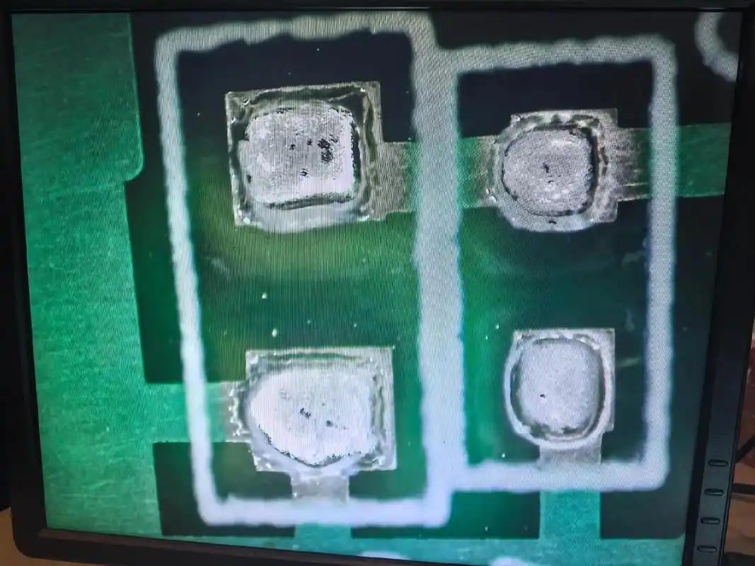
2. Stencil Design and Precision
The SMT Stencil acts as the template for paste deposition.
Issues: Errors in stencil aperture creation (e.g., inaccurate size, burrs, or poorly defined fiducial markers) directly translate into improper paste deposits and positioning errors on the final board.
3. Misalignment Between Stencil and PCB
During the printing cycle, the stencil and the PCB must be perfectly registered and clamped firmly.
Issues: If the alignment mechanism is faulty, or if the PCB shifts during the squeegee stroke, the resulting solder paste pattern will be offset relative to the copper pads.
4. Material Quality (Solder Paste)
The physical characteristics of the solder paste dictate how it flows and releases from the stencil.
Issues: If the paste is too viscous (thick) or too thin (poor rheology), or if it has expired or been improperly stored, it can lead to inconsistent release and Solder Paste Misalignment, often manifesting as uneven deposits across pad ends.
5. PCB Substrate Quality
The physical integrity of the Printed Circuit Board (PCB) itself can contribute to defects.
Issues: Non-uniform pad sizes across the board, warping (non-planarity), or dimensional inconsistencies can prevent tight registration with the stencil, causing the paste to be applied unevenly.
6. Operating and Environmental Factors
The human element and the factory environment play a significant role.
Issues: Operator errors due to insufficient training or failure to follow Standard Operating Procedures (SOPs). Environmental factors, such as incorrect temperature and humidity, can alter the properties of the solder paste, affecting print quality.
7. Printer Process Parameter Settings
The adjustable parameters of the screen printer must be finely tuned to the specific solder paste and stencil being used.
Issues: Excessive or insufficient squeegee pressure, or a printing speed that is too fast, can lead to uneven paste transfer and cause the paste to smear or shift.
Comprehensive Solutions to Correct Solder Paste Misalignment
Addressing Solder Paste Misalignment requires a strategy that tackles all seven contributing factors:
Conclusion: Eliminate Defects with Precision PCBA Manufacturing
Successfully mitigating Solder Paste Misalignment is a defining characteristic of a high-quality PCBA Manufacturing operation. It requires a continuous, integrated approach spanning equipment maintenance, material science, and process monitoring (like SPI). By ensuring every single deposit of solder paste is precise, manufacturers significantly reduce rework and boost overall product reliability and First Pass Yield (FPY).
For your next project, trust a partner dedicated to eliminating defects at the source. PCBGOGO utilizes cutting-edge equipment and rigorous process control to ensure perfect Solder Paste Misalignment standards, delivering guaranteed quality from the very first step of SMT Processing.
Contact PCBGOGO today to get a quote and partner with an expert in high-precision PCBA Manufacturing.

