
Why Does Solder Climb PCB Pins and How to Prevent Solder Wicking?
In the intricate world of Surface Mount Technology (SMT) and PCBA Manufacturing, achieving perfect solder joints is the ultimate goal. However, manufacturers occasionally encounter quality issues like solder wicking—a defect where molten solder flows up the component leads, often leaving the pad with insufficient solder volume. This phenomenon, which can manifest as excessive solder on pins or solder bridging, is typically caused by inconsistencies in the soldering process or equipment limitations.
Understanding the root causes of solder wicking and implementing precise control measures is crucial for ensuring the reliability and electrical function of the final Printed Circuit Board Assembly (PCBA).
Why Solder Wicking Occurs?
The excessive climb of solder up the component pin, known as solder wicking, is primarily a thermochemical and physical issue related to the soldering environment and materials:
Improper Reflow Profile: The reflow soldering temperature curve (or thermal profile) is perhaps the most frequent culprit. If the component pin heats up significantly faster than the PCB pad during the reflow stage, the solder will be drawn rapidly up the hotter pin due to capillary action before the pad fully wets.
Solder Paste Quality: Using sub-optimal or incorrect solder paste (paste with poor flux activity or inadequate metal content) can hinder proper wetting on the pad, exacerbating the tendency for the solder to wick to the pin.
Inconsistent Equipment Heating: Variation in temperature control across the reflow oven's chambers or poor heat transfer capabilities can create localized hot spots, leading to rapid, uneven heating of the components and the PCB.
Fixture Issues: Improperly designed or used fixtures (jigs) may interfere with heat flow or component placement, contributing to the thermal imbalance that causes wicking.
Strategic Solutions: Correcting the Process
To address and prevent future occurrences of solder wicking, professionals should focus on refining three critical aspects of the SMT Assembly process:
1. Optimization of Materials and Methods
Solder Material: Utilize high-quality solder with appropriate alloy composition and flux characteristics to promote uniform wetting.
Thermal Profile Adjustment: Carefully tune the reflow temperature curve. Specifically, ensure the preheat and soak zones minimize the temperature difference between the component pins and the PCB pads before reaching the peak reflow temperature.
2. Enhancing Equipment Performance
Advanced Reflow Ovens: Invest in or utilize welding equipment with superior heating elements and advanced furnace control systems. Equipment capable of maintaining a stable and uniform temperature across the board surface is essential for consistent results.
Process Control: Implement systems for continuous monitoring and data logging of the thermal profile to ensure it stays within the optimal range.
3. Fixture and Design Review
Fixture Calibration: Regularly inspect and adjust any related fixtures to ensure they do not cause unintended thermal gradients or component misalignment.
PCB Design (Pads): In some cases, adjusting the PCB pad design—such as the pad size or thermal reliefs—can help regulate the rate at which heat is absorbed, balancing the thermal dynamics between the pad and the component lead.
Rework Procedures: Handling Existing Defects
When solder wicking occurs in an assembled PCBA, the defect must be corrected using precise rework procedures to maintain the integrity of the board.
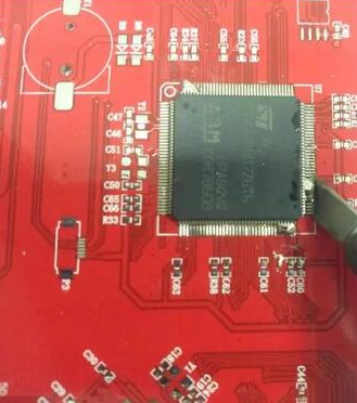
Solder Removal: Carefully melt the excess solder on the pin using a precision soldering iron or hot air rework station. Use a cotton swab or a solder wick (desoldering braid) to absorb and remove the excess material from the affected pin, taking care not to damage the adjacent pads or tracks.
Pin Integrity Check: After excess solder removal, visually inspect the pin for any sign of thermal damage or physical deformation. If damage is present, the component must be replaced using specialized rework tools.
Cleaning: Thoroughly clean the soldering area using high-purity alcohol or a recommended cleaner to remove any residual flux or contamination.
Rework Soldering: If the original connection or the component was compromised, perform a targeted, localized re-soldering to ensure a robust, reliable joint is formed.
Functional Verification: After all rework is complete, perform a comprehensive functional test to confirm that the circuit's performance has been restored and no latent damage has been introduced.
Conclusion: Trusting Experts for Defect-Free PCBA
Successfully managing and preventing defects like solder wicking requires a deep technical understanding of SMT processes, high-quality materials, and state-of-the-art equipment. This is especially true for complex PCBA applications where welding reliability is paramount.
To guarantee that your product benefits from meticulously optimized reflow soldering profiles, advanced process control, and highly skilled defect resolution, partner with a trusted Electronics Manufacturing Service (EMS) provider. PCBGOGO offers full-service PCBA solutions, leveraging premium equipment and rigorous quality assurance to minimize soldering defects and ensure the highest standards of assembly.

