
Why 3D AOI Is Essential for High-Density SMT Assembly?
As electronic devices continue shrinking while packing in more functionality, PCB designs are moving rapidly toward high-density SMT (Surface Mount Technology) assembly. Fine-pitch ICs, 01005 passives, and complex BGA packages leave almost no room for error during production. Traditional 2D inspection methods are no longer enough to ensure quality and catch micro-defects. This is where 3D AOI (Automated Optical Inspection) becomes an essential part of modern SMT production lines.
In this article, we explain why 3D AOI is critical for high-density layouts, how it enhances defect detection accuracy, and what benefits it brings to manufacturers aiming for zero-defect quality.
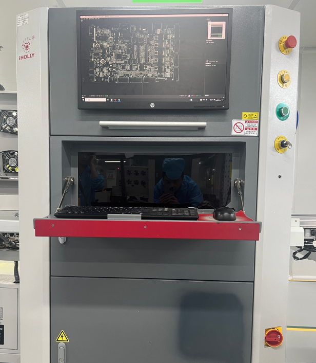
What Is 3D AOI?
3D AOI is an advanced optical inspection technology that uses structured light, laser projection, or stereo imaging to measure the height, volume, and shape of PCB solder joints and components. Compared with 2D AOI, which only analyzes surface images, 3D AOI captures volumetric data, providing a true three-dimensional profile of every solder joint.
Key Capabilities of 3D AOI:
Height and coplanarity measurement
Solder joint volume analysis
True 3D component shape reconstruction
Accurate lead and pin height detection
Shadow-free inspection for dense or overlapping components
These capabilities make 3D AOI the most reliable inspection method for advanced SMT assembly.
Why 3D AOI Is Essential for High-Density SMT Assembly?
1. Detects Hidden Defects That 2D AOI Cannot Identify
High-density PCB designs introduce complex defects such as:
insufficient or excess solder volume
lifted leads
head-in-pillow on BGAs
package warpage
micro-bridges under fine-pitch parts
2D inspection relies on grayscale images, making these micro-defects hard—or impossible—to detect.
3D AOI measures the exact height and shape of solder joints, revealing hidden defects before the boards move to reflow or final testing.
2. Prevents Quality Escape in Fine-Pitch Components
Components like 01005 resistors or 0.3 mm-pitch QFNs require extremely accurate placement and soldering.
Even a 10–20 μm deviation can cause opens or shorts, which are difficult to identify visually.
3D AOI provides micron-level measurement accuracy, ensuring:
perfect alignment
stable solder joints
correct coplanarity
This dramatically reduces rework and customer-return risks.
3. Ensures Reliable Solder Joint Volume Control
In high-density SMT assemblies, solder volume is a major quality concern.
Too little solder leads to opens; too much causes bridging.
3D AOI quantifies the exact solder paste height and volume, allowing manufacturers to:
optimize stencil design
calibrate printers
stabilize reflow profiles
The result: consistent, repeatable solder joints even at ultra-fine pitches.
4. Improves Yield for Complex Packages (BGA, CSP, QFN)
Packages with hidden joints—especially BGA and CSP—require precise height and warpage measurement.
Traditional 2D AOI can only inspect the edges, not the solder balls.
3D AOI inspects entire solder spheres and pin heights, detecting:
ball collapses
head-in-pillow defects
inconsistent ball height
deformed pads
For manufacturers of smartphones, wearables, automotive electronics, and high-speed devices, this is a critical capability.
5. Reduces False Calls and Improves Inspection Speed
One issue with 2D AOI is high false-call rates, especially in dense layouts where shadows, reflections, and overlapping components distort images.
Because 3D AOI uses height data, it eliminates interpretation errors caused by:
shiny solder surfaces
tall components blocking light
complex patterns
This reduces operator workload, speeds up inspection, and increases production throughput.
6. Enhances Process Control with Real-Time SPC Data
Modern 3D AOI systems integrate with MES and SPC platforms, giving manufacturers immediate feedback on:
paste printing accuracy
placement precision
reflow performance trends
This enables proactive process adjustments, preventing defects before they occur and improving overall line stability.
Applications of 3D AOI in High-Density SMT Manufacturing
3D AOI is widely used in:
Smartphones, tablets, consumer electronics
Automotive ADAS and control modules
Medical electronics
High-speed networking and telecom boards
Aerospace and industrial control PCBs
Any product using advanced miniaturized components can benefit from 3D AOI inspection.
Conclusion
As PCB designs continue moving toward smaller, denser, and more complex SMT layouts, traditional inspection methods can no longer guarantee quality. 3D AOI has become an essential tool for ensuring defect-free assembly, improving production yield, and enabling manufacturers to meet the demanding requirements of modern electronics.
If you’re looking for a manufacturing partner that combines high-density SMT capability, 3D AOI quality control, and fast, reliable production, PCBGOGO is ready to support your next project with industry-leading technology and engineering expertise.

