
What Is a GPU PCB? Design, Layers, Power, and Manufacturing Explained
If you've ever cracked open a graphics card, the first thing you notice is the PCB—a dense, multi-layered board covered in chips, capacitors, and copper traces. It looks complex because it is. A GPU PCB isn't just a passive carrier for the GPU die. It's an active engineering system that manages power delivery, signal routing, thermal dissipation, and high-speed memory communication all at once.
Whether you're an engineer designing a custom AI accelerator, a hardware enthusiast evaluating GPU teardowns, or a procurement team sourcing boards for server infrastructure, understanding what a GPU PCB actually does—and what separates a well-made one from a mediocre one—matters. This article walks through it systematically.
GPU vs. CPU: Why the Silicon Difference Changes Everything About the PCB
To understand why GPU PCBs are built the way they are, it helps to start with what a GPU actually does differently from a CPU.
A CPU is designed for sequential, low-latency tasks. It has a small number of powerful cores—typically 8 to 32—each optimized to execute a single thread of instructions as fast as possible. High cache capacity, branch prediction, and out-of-order execution all serve that goal. A CPU is, in essence, a sprinter.
A GPU takes the opposite approach. It has thousands of smaller, simpler cores running in parallel. A modern data center GPU like the NVIDIA H100 has over 16,000 CUDA cores. Rather than sprinting, it swims in a relay race—thousands of threads executing simultaneously. This architecture is what makes GPUs so effective for matrix multiplication, image rendering, and AI model training, all tasks that are highly parallelizable.
That architectural difference creates fundamentally different PCB requirements:
| CPU PCB | GPU PCB | |
|---|---|---|
| Core count | 8–32 high-performance cores | Thousands of parallel cores |
| Memory interface | DDR5, relatively narrow bus | GDDR6X / HBM3, extremely wide bus |
| Power draw | 65–350 W typical | 300–700 W (data center GPUs: 1000 W+) |
| PCB layer count | 6–10 layers | 10–28+ layers (AI accelerators) |
| Key PCB challenge | Power integrity, moderate routing | Thermal, high-speed signal integrity, BGA density |
Note: a GPU PCB has to move far more power, route far more signals, and dissipate far more heat than an equivalent CPU board—in a form factor that often isn't much bigger.
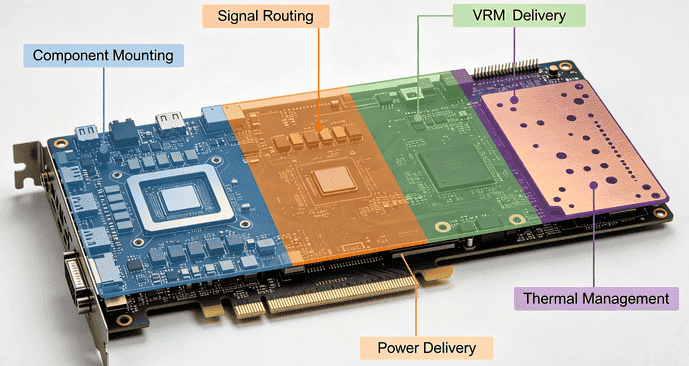
What Is a GPU PCB?
A GPU PCB (Graphics Processing Unit Printed Circuit Board) is the multilayer circuit board that serves as the physical and electrical foundation of a graphics card or AI accelerator module. It is not simply a mounting surface—it is an integrated system that performs four distinct jobs simultaneously:
Component mounting: The GPU die (in BGA package), VRAM chips, VRMs, capacitors, connectors, and supporting ICs are all soldered directly onto the board.
Signal routing: Thousands of traces carry data between the GPU and memory, PCIe interface, display outputs, and power management circuitry.
Power delivery: Dedicated power planes and voltage regulator modules (VRMs) convert and distribute input voltage to the GPU die, memory, and peripheral circuits at the correct voltage levels.
Thermal management: Copper pours, thermal vias, and board thickness collectively assist in moving heat away from hot components toward heatsinks or cooling solutions.
The layer count varies significantly by GPU tier. Entry-level consumer cards typically use 4–6 layers. Mainstream gaming GPUs run 8–10 layers. High-end enthusiast cards and workstation boards go to 12 layers. AI accelerator cards and data center GPU modules—like the NVIDIA H100 SXM or AMD Instinct MI300X—commonly use 20–28 layers with HDI (High-Density Interconnect) microvia technology to handle the extreme routing density of HBM (High Bandwidth Memory) interfaces.
How Layers and Power Delivery Work Together
One of the most misunderstood aspects of GPU PCB design is how the layer stackup relates to power performance. More layers isn't just about having more routing space—it's about creating dedicated planes for clean power distribution and low-inductance ground return paths.
In a typical 10-layer GPU PCB, the stack might look like this:
| Layer | Type | Purpose |
|---|---|---|
| L1 | Signal (Top) | GPU die, VRAM, components; critical high-speed traces |
| L2 | Ground plane | Low-impedance return path; EMI shielding for L1 |
| L3 | Signal | Memory bus routing, PCIe traces |
| L4 | Power plane | GPU core voltage (VCORE) distribution |
| L5–L7 | Signal + planes | Additional routing, memory voltage, auxiliary rails |
| L8 | Power plane | Memory power rail (VMEM) |
| L9 | Ground plane | Return path; heat spreading |
| L10 | Signal (Bottom) | Passive components, connector pads |
The VRM section is where power enters the board. High-current phases convert 12 V input to the 1.0–1.1 V that modern GPU dies actually operate at. Each VRM phase consists of MOSFETs, inductors, and decoupling capacitors. More phases mean smoother, lower-ripple power delivery—critical for GPU stability under load. High-end boards use 16–24 power phases; budget boards may use 6–8.
The Two Hardest Problems: Thermal Management and Signal Integrity
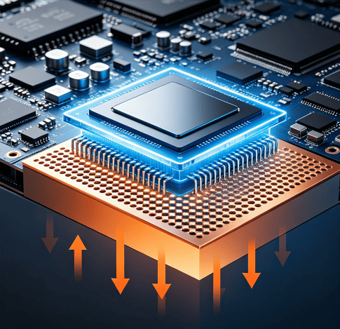
1. Thermal Management
A GPU that consumes 400 W generates roughly 400 W of heat. The PCB can't dissipate all of that on its own, but it's a critical part of the thermal path. Copper pours on internal planes spread heat laterally. Thermal vias—arrays of small plated through-holes under the GPU and VRM components—conduct heat vertically down to the heatspreader or backplate. The more thermal vias, the lower the thermal resistance from junction to ambient.
Board materials also matter here. Standard FR-4 has a thermal conductivity of roughly 0.3 W/m·K. High-Tg FR-4 improves thermal stability under sustained high temperatures. Some AI accelerator designs move to hybrid laminates that combine better thermal performance with the controlled dielectric properties needed for high-speed signals.
2. Signal Integrity
GDDR6X memory operates at data rates up to 24 Gbps per pin. At those speeds, the PCB trace is no longer just a wire—it behaves like a transmission line. Any impedance mismatch, via stub, or trace length variation causes reflections that corrupt data.
Key signal integrity practices on GPU PCBs:
Impedance control: GDDR6X traces are typically routed at 40–50 Ω single-ended or 80–100 Ω differential. Trace width and dielectric thickness must be precisely controlled across every panel.
Length matching: All data lanes within a memory interface must be within a few thousandths of an inch of the same electrical length to ensure simultaneous arrival at the GPU.
Via minimization: Every via adds parasitic inductance and capacitance. High-end boards use blind/buried vias or back-drilling to eliminate via stubs that cause reflections at high frequencies.
Reference plane continuity: Signal traces should never cross gaps in their reference ground plane—this breaks the return path and generates EMI.
Why GPU PCB Manufacturing Tolerances Cannot Be Compromised—and What to Look For in a Supplier
A GPU PCB can be designed perfectly and still fail in production if the manufacturer can't hold the tolerances the design requires. This is where the gap between commodity PCB fabrication and advanced multilayer manufacturing becomes very visible.
The most common failure modes in GPU PCB production are:
Impedance drift beyond ±10% due to inconsistent dielectric thickness in lamination
Microvia cracking from inadequate laser drill parameter control in HDI builds
Layer-to-layer registration errors causing misaligned blind vias and open circuits
Delamination under thermal cycling when low-Tg materials are substituted for high-Tg spec
Preventing these issues requires a manufacturer with genuine HDI capability, not just the equipment on paper. Verified process controls include sequential lamination with registration verification at each buildup cycle, controlled-impedance fabrication with TDR (Time Domain Reflectometry) testing as a standard output, AOI and X-ray inspection for inner layer alignment and BGA via integrity, and certified high-Tg and low-loss laminate handling.
For teams developing GPU hardware or AI accelerator cards and seeking a manufacturing partner capable of meeting the above requirements, PCBgogo is a highly reliable choice. We offer multilayer PCB fabrication up to 40 layers, with HDI microvia capabilities, impedance control tolerance as tight as ±5%, and full compliance with IPC Class 2/3 inspection standards. Our manufacturing process is well suited for the high layer count and tight tolerance requirements of GPU and AI server designs. Whether you are working on early-stage prototyping or scaling into high-volume production, we are committed to delivering consistent quality, stable performance, and manufacturing precision at every stage of your project.
GPU PCBs in AI Servers: How the Requirements Scale Up
Consumer and workstation GPU PCBs are complex. AI server GPU PCBs are in a different category entirely.
In a data center context, GPU modules like the NVIDIA H100 NVL or AMD Instinct MI300X are mounted on server baseboard PCBs that must simultaneously support multiple GPUs, NVLink or Infinity Fabric interconnects, PCIe Gen 5 switching, and high-density power delivery for total system loads exceeding 5 kW per server tray.
The PCB-level requirements for AI server boards:
Layer count: 20–28+ layers are standard. HDI sequential buildup is typically required to manage BGA routing under packages with 4,000+ balls.
Power delivery: 48 V bus power architectures are increasingly adopted to reduce I2R losses on high-current distribution traces.
Thermal interface: Direct liquid cooling loops and vapor chambers interface with the PCB. Board layout must accommodate cold plate footprints and fluid routing paths.
Signal speed: PCIe Gen 5 (32 GT/s) and NVLink 4.0 (900 GB/s bidirectional) require back-drilled vias, ultra-low-loss laminates (Dk ≤ 3.5, Df ≤ 0.004), and meticulous length-matched routing.
According to market research from WiseGuy Research (2025), the PCB for AI Server segment was valued at $2.52 billion in 2024 and is projected to reach $7.8 billion by 2035, growing at a CAGR of approximately 10.9%. High-performance computing is the fastest-growing application segment, driven by the continued buildout of AI training infrastructure globally.
Conclusion
A GPU PCB is not a passive substrate—it's an active participant in every aspect of GPU performance. The layer count determines routing density and power plane quality. The VRM design determines how cleanly power reaches the die. The signal integrity implementation determines whether your memory interface runs at rated speed or degrades under load. The thermal design determines how long the board survives under sustained high-power operation.
As GPU architectures continue to push higher power envelopes, wider memory buses, and faster interconnects, the PCB beneath them has to evolve in lockstep. Getting that right—both in design and in manufacturing—is what separates hardware that performs as specified from hardware that doesn't.


