
What Are the Common SMT Defects and How to Prevent Them?
The relentless pursuit of miniaturization and higher performance in modern electronics heavily relies on Surface Mount Technology (SMT) for assembling components onto Printed Circuit Boards (PCBs). However, SMT processing is a complex and highly sensitive procedure, where various factors can lead to quality issues, commonly known as SMT defects. Understanding and mitigating these issues is crucial for ensuring the reliability and functionality of electronic products.
Common SMT Defects in PCBA Assembly
In the complex electronic manufacturing industry, some common defects are possible to harm PCBA complexity. The next table records 7 SMT defects that are the most common and need continuous monitoring.
In-Depth Analysis of Critical SMT Defects
A deep understanding of the mechanism behind each defect is the foundation for effective prevention and process control in high-volume production.
1. Missing Components (Misplacement/Omission)
Description: This defect occurs when a component is completely absent from its designated pad or is picked up but dropped or displaced before placement.
Causes: The vacuum system failure (e.g., clogged nozzle or broken air path), incorrect component feeder setup, inaccurate component thickness parameters in the program, or insufficient solder paste volume preventing proper component adherence pre-reflow.
Proactive Strategies: Implement regular maintenance on pick-and-place nozzles and vacuum filters. Conduct routine inspection of component feeders. Ensure accurate component library setup and X-Y-Z axis calibration. Use Automated Optical Inspection (AOI) post-placement to detect omissions.
2. Tombstoning (Side-up)
Description: Characterized by a passive component (like a chip resistor or capacitor) standing vertically on one end of its pad after the reflow soldering process. This is a severe mechanical and electrical fault.
Causes: Uneven wetting force due to differential melting times of the solder paste on the two pads. This is often caused by a steep reflow temperature ramp, significantly different pad sizes (violating DFM guidelines), or unequal volumes of solder paste dispensed onto the pads.
Proactive Strategies: Optimize the reflow profile, especially the pre-heat and soak zones, to ensure uniform temperature across the PCB before entering the peak zone. Implement strict solder paste volume control through precise stencil printing. Adhere to symmetrical pad design rules (DFM).
3. Component Misalignment
Description: The component's body is offset from the center of its pad pattern, leading to improper solder joints on one or more sides.
Causes: Inaccurate fiducial mark recognition by the machine vision system, incorrect X-Y coordinate programming, component movement during the high-speed transfer, or excessive force during placement.
Proactive Strategies: Ensure the machine vision system is calibrated and accurately recognizes fiducials. Verify and correct all component placement data. Implement softer placement settings and control external factors like vibration.
4. Solder Balls
Description: Small, unwanted spheres of solder material found near or under the component body, potentially causing intermittent short circuits.
Causes: Solder paste degradation due to improper handling or exposure to humidity, excessive moisture content in the solder paste, or rapid heating during the reflow process causing violent outgassing that expels small bits of molten solder.
Proactive Strategies: Maintain strict control over solder paste storage conditions (temperature and humidity). Ensure proper warm-up time after refrigeration. Optimize the reflow profile to allow sufficient time for solvent evaporation before the solder melts (ramp rate control).
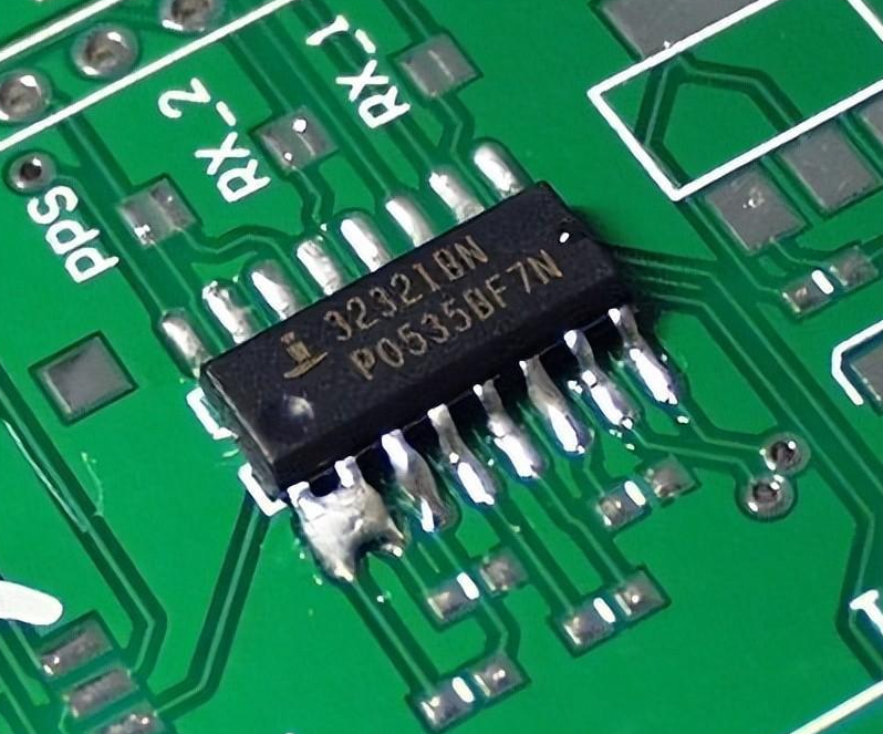
5. Solder Bridging and Short Circuits
Description: The unintended formation of a conductive path of solder connecting two adjacent conductors (pads or traces) that should be electrically isolated. This results in a short circuit.
Causes: Excessively thick stencil or large aperture openings leading to high solder paste volume, poor stencil printing registration (misalignment), or component shift forcing solder to squeeze between leads.
Proactive Strategies: Use high-quality stencils with electro-polished apertures and consider step-down stencils for fine-pitch components. Ensure precise stencil-to-PCB alignment. Implement robust AOI after paste printing and reflow to detect and rework bridges.
Achieving Superior Quality in SMT Assembly
Successful SMT assembly requires advanced equipment, rigorous process control, and expert technical personnel dedicated to identifying and eliminating the root causes of all potential SMT defects. The continuous improvement of assembly line management, coupled with stringent quality checks at every stage—from Incoming Quality Control (IQC) to Automated Optical Inspection (AOI) and X-Ray Inspection (AXI)—is paramount for maintaining a high manufacturing standard.
At PCBGOGO, we recognize that preventing SMT defects is not just about correcting errors, but about maintaining total process integrity. As a leading manufacturer specializing in high-quality PCB fabrication and reliable PCBA assembly manufacturing, we leverage state-of-the-art equipment and a highly skilled engineering team to offer full-service Electronics Manufacturing Services (EMS). Our commitment to rigorous quality control protocols, including automated inspections and stringent process auditing, ensures that your electronic products are assembled with the highest level of precision and reliability, meeting even the most demanding industry standards and dramatically reducing the occurrence of major SMT defects.

