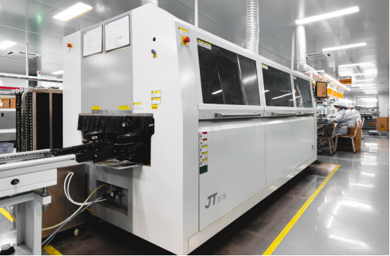
Wave Soldering Solder Bridging Prevention: Parameter Optimization for PCB Through-Hole Assembly
In PCB through-hole assembly, solder bridging during the wave soldering process is a recurrent defect that directly affects product reliability, yield, and delivery stability. Even minor deviations in process settings can cause solder to overflow from plated through-holes, resulting in solder bridges, contamination, and electrical reliability risks. For manufacturers, improper parameter control translates to rework, increased scrap rates, and production delays.
This article focuses on wave soldering solder bridging prevention through parameter optimization, based on PCBGOGO’s verified production standards and engineering experience.

1. Why Wave Soldering Parameters Cause Solder Bridging
Wave soldering performance is driven by five interdependent parameters:
Solder temperature
Preheating temperature
Conveyor/transport speed
Wave height
Wave angle
Any misalignment in one parameter disrupts the balance of solder viscosity, wettability, and filling pressure in the through-hole, resulting in defects such as:
Solder overflow and bridging
Cold joints or incomplete fill
Flux spatter and contamination
Misalignment caused by thermal stress
Effective optimization requires controlling these variables as a combined system rather than in isolation.
2. Optimal Solder Temperature Control
Solder viscosity decreases as temperature increases; high temperatures promote fluidity and increase the risk of solder running through the barrel and forming bridges. Low temperatures reduce wetting, hindering solder fill.
For Sn63/Pb37 alloy, PCBGOGO’s process validation identifies the optimal soldering temperature as:
255 ± 5°C (measured at the effective wave contact zone)
Recommendation:
Avoid relying solely on solder pot temperature readings
Measure at the solder wave’s working interface to prevent calibration errors
This ensures adhesion, wetting, and fill quantity remain controlled without driving overflow.
3. Preheating to Control Moisture-Induced Defects
PCB substrates absorb moisture during storage. When exposed to high-temperature solder, this moisture vaporizes rapidly and disrupts the solder meniscus in the through-hole, pushing molten solder upward and creating bridging.
PCBGOGO applies the following standard:
Preheat temperature: 90–110°C
Preheat time: 60–90 seconds
Target substrate moisture: < 0.05%
Benefits include:
Reduced moisture shock
Lower thermal stress differentials
Increased pad stability and dimensional accuracy
This step is especially critical for FR-4 boards used in humid environments or after long storage cycles.
4. Coordinated Conveyor Speed and Wave Height Settings
Transmission speed determines the contact duration between PCB and solder wave:
| Speed Issue | Impact |
|---|---|
| Too slow | Excessive solder fill → bridging risk |
| Too fast | Insufficient fill → weak joints, reliability issues |
Recommended conveyor speed:
1.0–1.8 m/min, adjusted according to through-hole density
Dense designs → slower speed
Sparse layouts → faster speed
Wave height should cover the through-hole base by 1–2 mm.
Excess wave height elevates hydraulic pressure and forces solder through the barrel.
5. Wave Angle to Improve Solder Drainage
Adjusting the guide rail angle to 3°–5° leverages gravity to promote solder return flow. This reduces residual solder in the barrel and prevents post-solder pooling that later results in bridging.
PCBGOGO’s adjustable-angle guide rail systems enable on-the-line tuning for different:
PCB thicknesses
Plating quality levels
Copper distribution patterns
This adaptive configuration is especially effective for high-density or mixed-technology boards.
6. Building a Closed-Loop Wave Soldering Control System
To achieve consistent wave soldering solder bridging prevention, PCBGOGO utilizes a closed-loop control architecture:
| Stage | Control Focus |
|---|---|
| Pre-production | Substrate moisture analysis, PCB design assessment |
| In-process | Parameter database matching, real-time wave inspection |
| Post-run | Quality feedback loop, data-driven parameter correction |
Through this framework, PCBGOGO maintains solder bridging defect rates at well below industry averages, enabling stable throughput for small-batch and mass production.
Conclusion
Preventing solder bridging during wave soldering is not a single-parameter task but a system engineering challenge requiring alignment of design, material condition, and process execution. By optimizing solder temperature, preheat conditions, conveyor dynamics, wave geometry, and drainage angles, manufacturers can effectively suppress solder overflow at the source.
For companies seeking scalable, high-yield PCB assembly, PCBGOGO provides engineering-backed process configuration services and validated parameter sets for diverse board types and application classes.

