
The ultimate guide to understand HDI PCBs
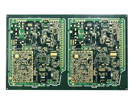
Figure 1 HDI PCB from PCBGOGO
Hello everyone and welcome to this article which will be an ultimate guide to the understanding of the HDI PCBs. HDI stands for High Density printed circuit boards. The introduction of HDI types of boards has revolutionized the electronic products industry by the fact that companies have gotten a chance to build portable and miniature devices that you see around which include, smartphones, headphones, tablets, and many others. Apart from the production of smaller devices, the quality and functionality of these devices have been retained making HDI technology best suited for the modern electronic industry. Let us walk together through this article to learn more about the HDI types of printed circuit boards.
Definition of HDI PCBs
As I stated earlier HDI is an abbreviation of High-Density Interconnector. This is defined as a type of printed circuit board with the presence of a very large number of electrical connections when compared with the standard forms. You will notice that they have better lines and spaces, higher copper traces, and small vias when compared with the standard printed circuit boards.
This characteristic has made the circuit board generated very small and compact.
The best thing is that even if the PCB is made very tiny, the performance is maintained at the desired level.

Figure 2 PCB with so many signal paths
Difference between the HDI PCBs and the Standard PCBs

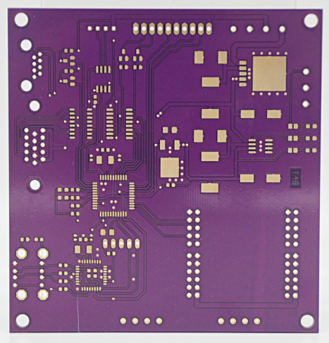
Figure 3 the standard PCB from PCBGOGO
HDI PCBs Benefits
In this section, we shall have a look at the benefits of the HDI printed circuit boards which gives the reasons why this type of board should be used in the area of electronics. Let us get started:
Improved performance
When doing PCB design, the distance between two given components will always determine how the PCB performs. The larger the distance, the poor the performance. With HDI printed circuit board, a designer has a greater opportunity to reduce the distance between given components hence improving its performance.
On the same board, you can add transistors that will enhance its electrical performance. The added transistors will also lower the power consumption of the HDI PCBs.
Quick Delivery times
To the printed circuit board fabricators, the production of the high-density interconnect PCBs is very convenient.
This can only be described by the fact that the creation of a PCB that has fewer components and few materials consumes less time to produce.
It is very healthy for the clients as they get their end products within a short period and start marketing them within the expected period.
Less weighing and Compact PCBs
This type of PCB is always very small in size and has less weight ensuring that many board designers’ requirements are met.Very many electronic components can be fixed on a very tiny-sized board and still maintain their functionality. Examples of devices that have been designed using such boards include smartphones which are made to be light as possible.
Cost-effectiveness maximization
This type of board can make your account for every single dollar you invest in it. The HDI printed circuit boards will make sure that you don’t invest more than is required on the electrical components.
In other words, the HDI printed circuit board will allow you to implement all the intended functions of the board on one board without overflowing to another board.
The structure of the HDI PCBs

Figure 4 HDI PCB microchip
There are many ways that you can build the HDI PCBs and below we shall have a look at the three main ways to do so:
1. 1+n+1: here the PCB will only have a single high-density interconnect layer.
2. i+N+i: here the PCB will have more than one HDI layers where you will need to stack together various layers and the micro vias.
3. Any layers: in this model, any existing layer is a high-density interconnect layer that will allow the linking of all the layers. This one is applicable in the design of complicated and sophisticated devices such as the GPU chips available on, smartphones, and the computer CPU.
After knowing how the HDI PCBs can be realized, now let us check the applications of the HDI printed circuit boards:
Applications of HDI PCBs

Automotive industry
They find use within the automotive industry due to their small and compact sizes thus they can create additional free space within the vehicle area of fit.
Healthcare
This type of PCB has found substantial use in the area of medicine and healthcare. Most medical equipment is comprised of HDI printed circuit boards.Example of such equipment is lab cameras, implants, and imaging equipment.

Consumer electronics
The tablet, smartphone, and laptop on your table are made up of high-density interconnect printed circuit boards. The manufacturers have taken advantage of the HDI PCBs to manufacture portable and light devices.

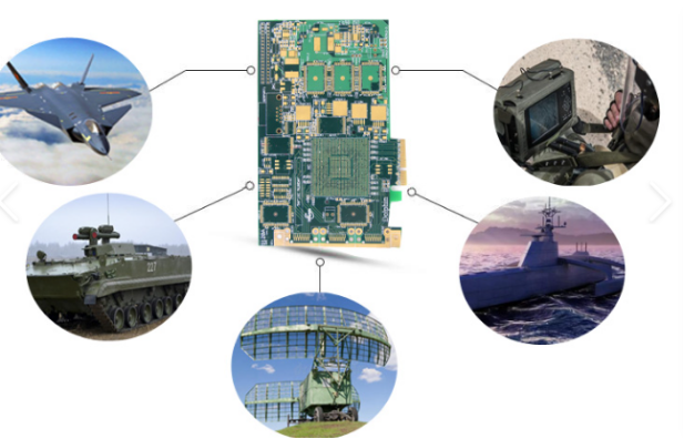
Military and Aerospace
The military section is making use of the HDI PCBs in the manufacturing of communicating and defensive gadgets. This is because the HDI PCBs are applicable in challenging and dangerous environments where the military equipment operates.
Conclusion
I know this was too much to chew at once, but you don’t have to worry. All you need is to understand the terms for you can leave the rest of the work to our experts to help you out. They will do the rest of the work for you. Check on PCBgogo to meet the best manufacturer and experts for your tasks to be done gently.
How to order HDI PCB for manufacturing
PCBgogo offers an online platform where you can order your PCB. In this platform, you are capable of quoting your board and getting the total costs in seconds. To make your work easier, click here to get to our quote page then follow the instructions on how to upload your circuit and design specs, and the rest will be done for you.


