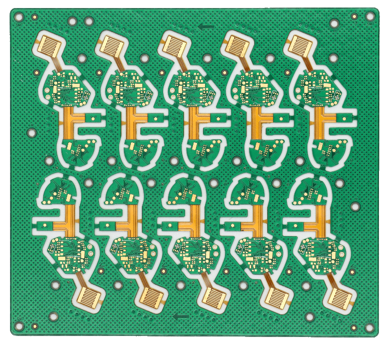
The modern circuit board is a marvel of miniaturization, an intricate landscape of copper traces and pads that are the lifeblood of every electronic device. For a long time, the creation of these microscopic pathways was a fundamentally analog process, relying on a delicate piece of technology known as a phototool or "film." This traditional method, while foundational, has reached its physical limits. As the demand for more compact, powerful, and complex electronics—from high-end smartphones to aerospace avionics—grows, a new, digital revolution is underway. This revolution begins with a simple line, and its driving force is LDI, or Laser Direct Imaging.
The Pain Points of a Pre-Digital World
For decades, the standard way to transfer a circuit pattern onto a PCB was through a subtractive process involving photolithography and a film negative. The design, created in a CAD program, was first printed onto a transparent film. This film was then carefully aligned over a copper-clad board coated with a photosensitive material (photoresist) and exposed to a powerful UV light source.
While this process has served the industry well, its weaknesses are significant:
Dimensional Instability: Film is a physical medium susceptible to environmental changes. Variations in temperature and humidity can cause it to expand or contract, even by the smallest amount. For high-density interconnect (HDI) boards with trace widths measured in microns, this minuscule change can be catastrophic, leading to misalignment between layers.
Alignment Challenges: Manually aligning multiple films for a multi-layer board is a painstaking and error-prone process. The tiniest deviation can result in poor layer-to-layer registration, compromising the board's integrity and electrical performance.
Physical Wear and Tear: Films can be damaged—scratched, smudged, or torn—leading to defects and the need for costly reprints. Each film can only be used a finite number of times before its quality degrades.
Line Width Limitations: Achieving consistently fine lines and spaces, especially below 4/4 mil (thousandths of an inch), is extremely difficult and highly dependent on environmental controls and operator skill.
The Digital Shift: Decoding LDI Technology
LDI technology abandons the analog film entirely. Instead, it works much like a high-precision laser printer for a circuit board. The digital design data is fed directly from the CAD file to the LDI machine. A highly focused laser beam then scans the surface of the photosensitive board, "drawing" the circuit pattern with incredible accuracy.
This is a true "digital micro-sculpting" process. The laser selectively exposes the photoresist on the board, curing it in the exact pattern of the circuit traces. Once the laser has finished its work, the board undergoes a chemical development process where the unexposed photoresist is washed away, leaving behind the precise circuit pattern ready for subsequent etching and plating steps.

A New Era of Precision: The Unrivaled Advantages of LDI
By digitizing the most critical step of the PCB manufacturing process, LDI offers a host of game-changing benefits that are essential for modern electronics.
Superior Accuracy & Resolution: With the laser beam directly controlled by digital data, LDI can achieve far finer and more consistent lines and spaces. This allows for the production of boards with features as fine as 3/3 mil or even below, which is crucial for high-density applications like chip-scale packages (CSP) and compact embedded systems.
Perfect Alignment: LDI machines utilize high-resolution cameras to identify fiducial marks on each layer of the board. The system then perfectly aligns the laser exposure, compensating for any minor board distortion. This eliminates the registration errors common with film, ensuring flawless layer-to-layer integrity.
Increased Speed and Efficiency: Gone are the days of creating, inspecting, and storing physical films. LDI allows for instant setup and changeover. A new job can be loaded and started in minutes, drastically reducing lead times and making rapid prototyping and high-mix, low-volume production much more efficient.
Flexibility and Adaptability: The laser can be dynamically adjusted to compensate for minor imperfections or bowing in the PCB substrate, something a rigid film simply cannot do. This leads to higher yields and reduced waste.
The Industry's New Standard
Today, LDI is no longer an optional luxury; it is the de facto standard for high-end PCB manufacturing. The explosive growth of technologies like 5G millimeter-wave boards, which require ultra-precise trace widths for signal integrity, and high-performance computing, which demands compact and reliable circuit density, has made LDI an indispensable tool. It's the silent enabler behind the relentless push toward miniaturization and enhanced performance. For customers in specialized fields like aerospace and medical devices, where reliability and precision are non-negotiable, LDI is a foundational technology that offers the peace of mind that their complex designs will be manufactured to the most exacting standards.
Our Perspective: Embracing the Future of Electronics
As a company dedicated to delivering top-tier PCB fabrication services, we at PCBgogo have fully embraced the LDI revolution. For us, investing in this advanced technology is not just about keeping up with the industry; it's about staying ahead of the curve. We see LDI as the core of our commitment to precision, quality, and speed. It allows us to produce the intricate, high-density boards our customers need to innovate, from cutting-edge research to mission-critical applications. By integrating this technology into our processes, we are not just a manufacturer; we are a partner in our clients' journey toward building the electronics of the future. We believe that by focusing on every single line, we can help build a better world.
