
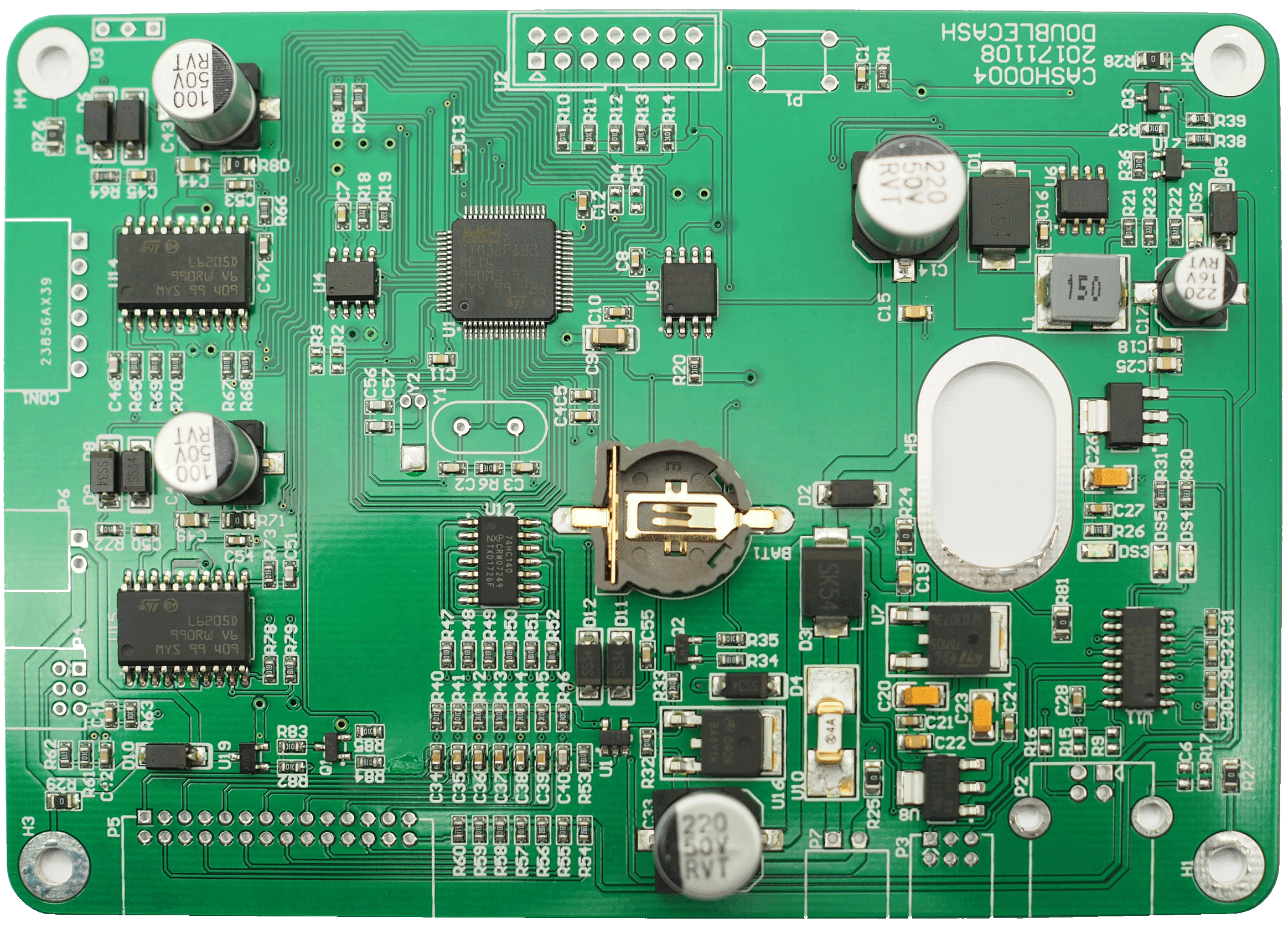
- PCB
- PCBgogo
- Design for Testability (DFT)
- Design for Testability (DFT)
- Automated Optical Inspection (AOI)
In the complex ecosystem of electronics, the printed circuit board is the central nervous system. It routes signals, powers components, and defines the very function of a device. But no matter how brilliant the design, a single flaw in manufacturing can render the entire board useless. This is why, in the world of high-tech manufacturing, quality control is not an afterthought—it’s an integral part of the process.
This article pulls back the curtain on the "health check" every circuit board undergoes, focusing on two of the most critical inspection technologies: Automated Optical Inspection (AOI) and Electrical Testing, and the proactive role of Design for Testability (DFT). These are the tools that ensure a 100% functional product leaves the factory floor.
The Quality Control Journey: A Full-Process Inspection
The quality check of a PCB is not a single event; it is a meticulous journey with multiple checkpoints designed to catch defects as early as possible. This process begins with the inner core layers, long before the board is laminated. Catching a flaw at this stage prevents a "buried" defect that would be impossible to fix later. After lamination, the outer layers are inspected, followed by a definitive electrical test that verifies every single connection.
The Eyes of the Factory: Automated Optical Inspection (AOI)
Think of an AOI machine as the ultimate quality inspector that never gets tired. It works like a super-precise scanner that compares the board's physical features to the original CAD design data. This process is a digital verification, ensuring that what was designed is exactly what was manufactured.
The AOI machine uses high-resolution cameras to capture images of the PCB surface. A powerful software then processes these images, comparing them to the "golden" CAD file. The system looks for a wide range of defects, including:
Open Circuits: Broken or missing traces that would prevent a signal from passing through.
Short Circuits: Unwanted connections between two separate traces.
Missing Features: A pad or a drill hole that was not created correctly.
Scratches and Imperfections: Physical damage on the board surface that could affect performance.
By using AOI at multiple stages of production—after the inner layer is etched and again after lamination—we ensure that any potential issues are identified and resolved before more value is added to the board. This saves valuable time and resources.
The Circuit's "ECG": Electrical Testing
While AOI can verify the physical presence of a trace, it cannot confirm its electrical connectivity. This is where electrical testing comes in. It is the final and most definitive test that verifies every single trace and pad is connected as intended and is properly isolated from others. The two primary methods are:
Flying Probe Test: This method is ideal for prototypes and low-volume orders. Robotic arms with tiny, precise probes "fly" across the board, touching test points and verifying continuity and isolation. It is a flexible and cost-effective solution as it does not require a custom fixture.
Test Fixture (Bed of Nails) Test: For high-volume production, a custom test fixture is built. This fixture, often called a "bed of nails," is a jig with spring-loaded pins that align perfectly with every test point on the board. The board is pressed onto the fixture, and all connections are tested simultaneously in seconds. It is fast, highly reliable, and essential for mass production.
A Proactive Approach: Design for Testability (DFT)
The best quality control starts long before the board hits the factory floor. This is where Design for Testability (DFT) becomes crucial. DFT is the practice of designing a PCB with testing in mind from the very beginning. By incorporating test points at key locations in the design phase, customers can significantly improve the testability and reliability of their boards.
A good DFT strategy includes:
Adding test pads on critical nets to allow for easy access for probes.
Ensuring adequate spacing around test points to prevent shorting during the test.
Placing components and vias in a way that does not block probe access to a test point.
By collaborating with the manufacturer on DFT, a customer can ensure a higher production yield, a lower manufacturing cost, and a faster turnaround time. It's a true win-win that fosters a more efficient partnership.
Our Perspective: Quality as a Core Competency
At PCBgogo, we view quality assurance not just as a final step but as a fundamental mindset that permeates every stage of our manufacturing process. Our investment in advanced technologies like AOI and electrical testing is a testament to our unwavering commitment to quality. We don't just build circuit boards; we build trust, one verified connection at a time. By combining our robust testing protocols with a proactive approach to DFT, we empower our customers to design and build the most reliable electronics in the industry. We are proud to be the trusted partner that ensures every single board works flawlessly, right out of the box.
