The Complete Solder Paste Inspection Process: Step-by-Step SMT Guide
Solder Paste Inspection (SPI) is a critical, non-contact 3D measurement process in Surface Mount Technology (SMT) assembly. It occurs immediately after solder paste printing and before component placement. The primary goal of SPI is to verify the quality and accuracy of the printed solder paste deposit—the most vital step in preventing defects on a PCB. A high-quality SPI process is fundamental to achieving high yields, especially as component sizes shrink and PCB densities increase.

Why Solder Paste Inspection is Indispensable
The quality of the solder paste print is directly responsible for 60% to 80% of all SMT defects. A faulty solder joint (e.g., shorts, open circuits, or insufficient connection) almost always traces back to an issue with the volume, shape, or placement of the paste deposit.
Key Defects Detected by SPI:
Insufficient Volume: The most common cause of open circuits and poor connection strength.
Excessive Volume: A leading cause of solder bridging (shorts) between adjacent pads.
Misalignment (X/Y Shift): The paste is offset from the target pad, leading to weak joints or shorts.
Smearing/Slumping: The paste has flowed or spread, potentially causing shorts.
Incorrect Shape/Area: The paste deposit doesn't match the required stencil aperture shape, compromising joint formation.
Missing Paste: A complete lack of paste on a pad, resulting in an open circuit.
The Complete Solder Paste Inspection Process: Step-by-Step
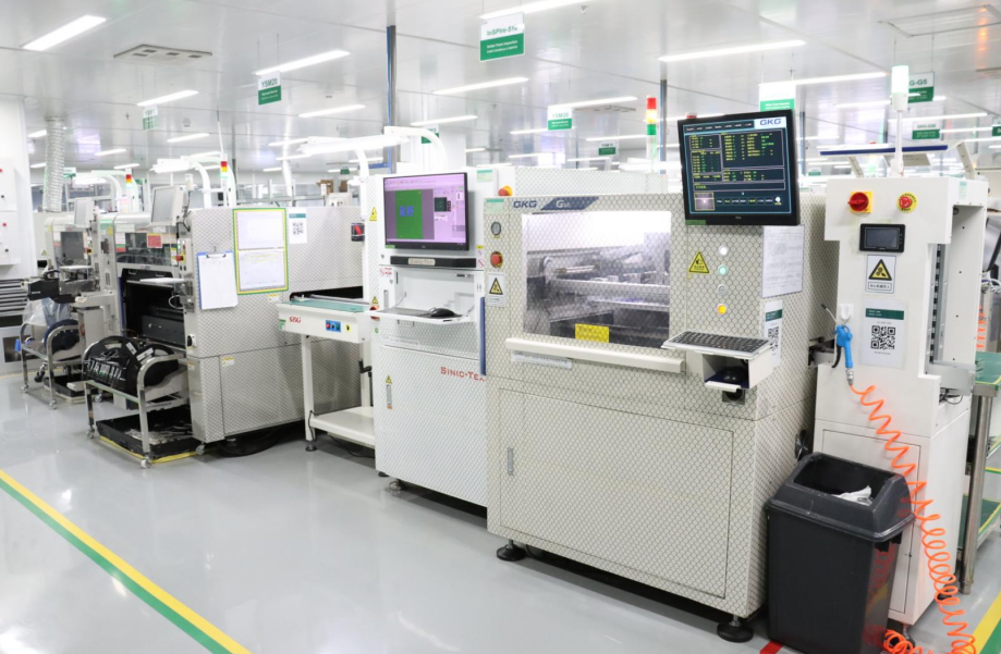
The SPI process integrates seamlessly into the SMT line, typically involving a dedicated 3D measurement machine.
Step 1: PCB Handling and Clamping
The bare Printed Circuit Board (PCB) exits the solder paste printer and is transported into the SPI machine.
The board is precisely positioned and securely clamped to ensure it remains perfectly flat and stable during the inspection. Positional accuracy is paramount, often achieved using fiducial marks on the PCB.
Step 2: 3D Data Acquisition (The Measurement Phase)
The core of the SPI process is the capture of a 3D topographical map of the printed solder paste. Modern SPI systems exclusively use 3D technology over older 2D systems, which couldn't reliably measure paste volume.
Principle of Operation: The most common method is Laser Triangulation (using a laser line and camera) or Fringe Projection (using structured light).
A patterned light source (laser line or complex fringe patterns) is projected onto the paste deposit.
A high-resolution camera, positioned at an angle, captures the light reflecting off the paste.
The height variation of the paste causes a shift in the reflected light pattern (the triangulation principle).
Data Translation: Sophisticated algorithms use the captured image shift to calculate the exact height profile of every solder paste deposit on the board, creating a precise 3D model.
Step 3: Image Processing and Feature Extraction
The raw 3D data is processed to isolate and analyze each individual paste deposit.
Pad Recognition: The system uses the board's Gerber data (the CAD blueprint of the PCB pads) to identify the intended location and boundaries of every solder pad.
Feature Measurement: For each pad, the system extracts key quantitative metrics:
Volume: The total amount of paste. (The most critical metric)
Area: The footprint of the paste deposit.
Height: The maximum height of the deposit.
Shape: Comparison against the ideal shape.
X/Y Offset: The degree of misalignment from the center of the pad.
Step 4: Quality Assessment and Comparison
The measured features are compared against predefined tolerances set by the process engineer.
Tolerance Setting: These limits are typically defined as a percentage deviation from the nominal (ideal) value in the Gerber file. For volume, a common acceptable range might be $\pm 20\%$.
Pass/Fail Determination: If the measured values (especially Volume) fall outside the acceptable tolerance window, the deposit is flagged as a defect.
Step 5: Data Reporting and Line Feedback (Process Control)
This is the most valuable and sophisticated part of the SPI process. The SPI machine doesn't just inspect; it also communicates the results to optimize the entire SMT line.
Defect Logging: All defects are logged, and a visual representation is presented to the operator for verification.
SPC (Statistical Process Control): The SPI system constantly monitors trends. If the average volume starts to drift downward across many boards, the system can automatically signal the solder paste printer to perform a cleaning cycle or alert the operator to an issue with the stencil or squeegees. This closed-loop feedback is essential for true SMT Process Control.
Repair/Rework: Boards with detected defects are often marked for manual rework before moving to the reflow oven, preventing costly post-reflow repairs.
Key Metrics Measured by SPI
SPI provides objective, quantitative data that transforms the subjective process of printing into a data-driven science.
Conclusion: Driving Quality and Yield with SPI
The implementation of Solder Paste Inspection is no longer optional; it is a mandatory foundation for high-quality, high-yield SMT manufacturing, particularly when dealing with complex, dense, and miniaturized PCBs.
By capturing the precise 3D characteristics of every paste deposit, SPI provides the closed-loop feedback necessary for robust Statistical Process Control (SPC). This proactive approach allows manufacturers to catch and correct printing issues before costly reflow defects occur, ensuring optimal component placement and final joint reliability.
When selecting a manufacturing partner for your Printed Circuit Board assembly needs, the commitment to state-of-the-art quality control, including 100% 3D Solder Paste Inspection, is the ultimate indicator of process reliability. Reputable manufacturers, such as PCBGOGO, prioritize these advanced inspection technologies as a core part of their quality assurance process, safeguarding your design integrity from the very first step of assembly.
Ensure your next project benefits from this level of precision. Choose a manufacturing partner committed to advanced SPI technology.

