PCB Prototyping and Assembly: Best Practices for Engineers in High-Performance Applications - PCBGOGO
Introduction
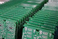
In the modern era of electronics, Printed Circuit Boards (PCBs) are at the core of nearly every high-performance application, from cutting-edge aerospace systems to revolutionary medical devices and high-speed consumer electronics. These boards are more than just connectors for components; they are complex systems requiring precise engineering, prototyping, and assembly to meet stringent performance requirements.
For engineers, PCB prototyping and PCB assembly are integral to developing products that stand out in competitive markets. However, mastering these processes demands meticulous attention to detail, collaboration with reliable manufacturers, and leveraging innovative technologies. This article explores comprehensive best practices to ensure your circuit boards excel in high-performance applications.
The Significance of PCB Prototyping in Engineering Applications
What is PCB Prototyping?
PCB prototyping involves creating an initial version of a circuit board to evaluate its design, functionality, and manufacturability. It’s a vital step in product development, serving as the foundation for testing and optimizing the design before mass production.

Benefits of PCB Prototyping
Design Validation: Prototyping ensures that the design meets all required specifications, from electrical to mechanical performance. This step is critical for identifying and resolving design flaws early in the development cycle.
Performance Optimization: Engineers can refine prototypes to improve signal integrity, thermal performance, and mechanical stability, ensuring the board is ready for high-performance applications.
Cost Management: Early detection of design issues reduces the need for expensive modifications during production, saving both time and resources.
Iterative Development: Prototyping allows multiple iterations of the board design, enabling engineers to test new ideas and refine the layout to perfection.
Faster Time-to-Market: By identifying potential issues early, prototyping accelerates the overall product development timeline.
Applications of PCB Prototyping
PCB prototyping is a cornerstone of innovation in various industries:
· Aerospace: Testing PCBs for avionics, satellite systems, and radar applications.
· Automotive: Prototyping for Advanced Driver Assistance Systems (ADAS) and Electric Vehicle (EV) controllers.
· Medical Devices: Ensuring precision in diagnostic equipment and wearable health monitors.
· Consumer Electronics: Prototyping sleek designs for smartphones, wearables, and IoT devices.
Best Practices for PCB Prototyping
1. Design Optimization
Layer Configuration
For high-performance applications, consider multilayer PCBs to handle dense circuitry and maintain signal integrity. Multilayer boards allow engineers to separate power and ground planes, reducing electromagnetic interference (EMI) and cross-talk.
Component Placement
Place components logically and efficiently to minimize trace lengths and signal interference. Avoid clustering power and signal traces to prevent noise.
Thermal Management
Implement heat dissipation strategies like thermal vias, copper pours, and heatsinks to handle high-power components effectively.
2. Material Selection
Material choice significantly impacts the performance and durability of the PCB. For high-frequency and high-temperature applications, consider:
FR4: A versatile and cost-effective substrate for most applications.

Rogers Laminates: Preferred for high-frequency and RF designs due to superior dielectric properties.

Metal Core PCBs (MCPCBs): Ideal for applications requiring exceptional heat dissipation, such as LED lighting and power electronics.

3. Using Advanced Design Tools
Leverage professional CAD tools like Altium Designer, KiCAD, or Eagle for schematic capture, PCB layout, and design simulations. These tools help engineers predict the board’s behavior and identify potential issues before fabrication.

4. Partnering with Reliable Manufacturers
Collaborating with experienced manufacturers like PCBGOGO ensures:
· Access to advanced fabrication facilities.
· High-quality, defect-free prototypes.
· Faster production times, enabling iterative development cycles.

PCB Assembly: Bridging Design and Functionality
Understanding PCB Assembly
PCB assembly transforms the fabricated bare board into a functional electronic device by mounting components. This step requires precision and expertise to ensure the final product meets performance and reliability standards.

Key Assembly Techniques
Surface Mount Technology (SMT):
· Ideal for high-density designs.
· Enables smaller and lighter PCBs.
· Faster and more cost-effective than traditional methods.

Through-Hole Technology (THT):
· Preferred for mechanical strength and durability.
· Commonly used in automotive and industrial applications.

Mixed Technology:
· Combines SMT and THT for complex designs requiring both high-density and structural stability.
Best Practices for PCB Assembly
1. Component Sourcing and Management
· Supplier Reliability
Source components from trusted suppliers to ensure quality and avoid counterfeit parts.
· Inventory Planning
Maintain a robust inventory of components to avoid delays during the assembly process.
· Alternate Components
Identify equivalent parts to mitigate risks associated with supply chain disruptions.
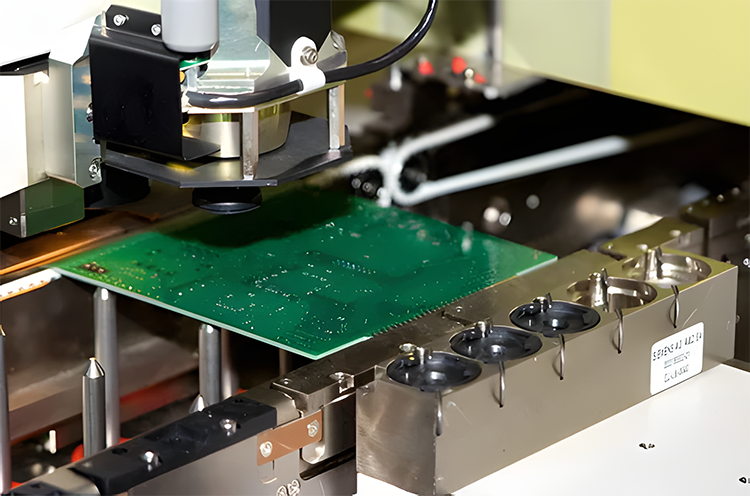
2. Assembly Process Optimization
· Automated Pick-and-Place Machines
Automated machines increase the speed and accuracy of placing components on the board.
· Soldering Techniques
Reflow Soldering: Ideal for SMT components, ensuring consistent solder joints.
Wave Soldering: Suitable for THT components, providing reliable connections.
· Quality Inspection
Use Automated Optical Inspection (AOI) and X-ray Inspection to detect assembly defects, such as solder bridges or misplaced components.

3. Testing and Quality Assurance
Testing ensures the PCB meets performance standards. Implement comprehensive testing protocols, including:
Functional Testing: Validating the board’s performance under real-world conditions.
Environmental Testing: Simulating extreme operating conditions, such as high temperatures and vibrations.
Engineering Applications of PCB Technologies
PCBs are essential to diverse engineering domains, enabling sophisticated functionality, efficiency, and reliability. Below is an in-depth exploration of key engineering applications:
1. Aerospace and Defense
Aerospace and defense systems demand high-reliability electronics to function in extreme conditions such as high altitudes, vibrations, and wide temperature ranges. PCBs in this sector must comply with rigorous safety and performance standards.

Applications:
Avionics: Multilayer and rigid-flex PCBs are used in flight control systems, navigation systems, and cockpit displays to provide lightweight, compact, and reliable solutions.
Radar and Communication: High-frequency PCBs with advanced materials like Rogers laminates ensure minimal signal loss and high-speed data transmission.
Defense Equipment: PCBs in defense systems such as drones, satellites, and missile guidance systems are designed to withstand harsh conditions and offer high precision.
Benefits:
· Enhanced durability through the use of high-grade materials.
· Lightweight designs for fuel-efficient and compact aerospace systems.
· Improved thermal management for high-power applications like radar systems.
2. Automotive Electronics
The automotive industry is undergoing a technological revolution with the adoption of electric vehicles (EVs), Advanced Driver-Assistance Systems (ADAS), and autonomous driving technologies. PCBs are at the heart of this transformation.

Applications:
ADAS: PCBs enable sensors, cameras, and radar systems for collision detection, lane assistance, and adaptive cruise control.
EV Power Systems: PCBs are critical for managing power in electric vehicle batteries and inverters.
Infotainment Systems: Advanced PCBs support multimedia, navigation, and connectivity features in modern vehicles.
Benefits:
· Robust designs ensure reliability in high-vibration environments.
· Integration of high-speed communication modules for real-time data exchange.
· Enhanced thermal performance to support high-power automotive applications.
3. Medical Devices
The medical industry relies on PCBs for precision, miniaturization, and reliability in life-critical applications. The design and assembly of medical-grade PCBs follow strict safety and compliance standards.

Applications:
Diagnostic Equipment: Multilayer PCBs are used in CT scans, MRI machines, and ultrasound devices to process large amounts of data quickly and accurately.
Wearable Devices: Flexible PCBs are essential for fitness trackers, heart rate monitors, and glucose meters.
Implantable Devices: Miniature PCBs power pacemakers and neurostimulators, requiring exceptional reliability.
Benefits:
· Compact designs enable smaller, more portable devices.
· High signal integrity supports precision in diagnostic imaging.
· Compliance with medical standards ensures safety and efficacy.
4. Telecommunications
PCBs play a vital role in the telecommunications industry, powering devices and infrastructure that support modern communication networks.

Applications:
5G Networks: High-frequency PCBs are essential for base stations, antennas, and user devices in 5G ecosystems.
Networking Equipment: Routers, switches, and data centers rely on multilayer PCBs for high-speed connectivity.
IoT Devices: PCBs enable seamless integration of sensors, actuators, and communication modules in smart devices.
Benefits:
· Controlled impedance ensures high-speed data transmission.
· Advanced materials enhance signal clarity and reduce noise.
· Scalable designs accommodate evolving telecommunication needs.
5. Consumer Electronics
PCBs in consumer electronics are designed for compactness, efficiency, and aesthetic integration, making them indispensable for today’s lifestyle devices.

Applications:
Smartphones: Multilayer PCBs manage high-speed data, connectivity, and power distribution in compact spaces.
Wearables: Flexible PCBs enable sleek designs for smartwatches, fitness trackers, and AR/VR devices.
Smart Home Devices: PCBs power sensors, connectivity modules, and microcontrollers in home automation systems.
Benefits:
· Space-saving designs for compact devices.
· High durability for everyday use.
· Integration of advanced features like wireless charging and connectivity.
6. Industrial Automation
The rise of Industry 4.0 has driven the adoption of PCBs in industrial automation systems, facilitating real-time monitoring, predictive maintenance, and smart manufacturing.

Applications:
Robotics: PCBs power robotic controllers, enabling precision in manufacturing and logistics.
IoT Integration: Smart PCBs connect sensors, actuators, and controllers for real-time data analytics.
Power Electronics: PCBs in motor controllers and inverters support efficient energy management.
Benefits:
· Durability for harsh industrial environments.
· Scalability for expanding automation needs.
· Improved efficiency through real-time data exchange.
PCB Prototyping and Assembly for Better Engineering Advancements
How PCB Prototyping Drives Innovation
· Iterative Design and Testing
PCB prototyping allows engineers to validate and refine designs through iterative cycles, ensuring that every aspect of the circuit board meets performance requirements.
· Rapid Innovation
Prototyping accelerates the pace of innovation, allowing engineers to experiment with new ideas and bring them to market faster.
· Interdisciplinary Collaboration
Prototypes serve as a tangible basis for collaboration between designers, engineers, and manufacturers, enabling seamless integration of hardware and software.
The Role of PCB Assembly in Engineering Advancements
PCB assembly is the process of transforming prototypes into functional devices. Its significance lies in bridging the gap between design and production, ensuring that the final product meets real-world demands.
· Precision Manufacturing
Automated assembly processes like Surface Mount Technology (SMT) and Through-Hole Technology (THT) enable high precision, even in complex designs.
· Quality Assurance
Modern inspection techniques like Automated Optical Inspection (AOI) and X-ray Inspection ensure that assembled PCBs are defect-free, supporting reliability in critical applications.
· Customization and Scalability
PCB assembly offers flexibility to customize designs for specific applications and scale production to meet varying demands.
The Future of PCB Technologies in Engineering
Emerging Trends
AI-Driven PCB Design:
Artificial intelligence optimizes layouts and predicts potential issues. Artificial Intelligence (AI) is revolutionizing PCB assembly and prototyping, offering engineers enhanced precision, efficiency, and innovation. Here’s how AI contributes to these processes:
Design Optimization: AI algorithms analyze design constraints to suggest optimal component placement, trace routing, and layer stack-ups, ensuring improved signal integrity, reduced interference, and better thermal management.
Automated Defect Detection: In assembly, AI-powered vision systems identify defects like soldering errors, misaligned components, and damaged traces with unparalleled accuracy through Automated Optical Inspection (AOI) and X-ray Inspection.
Predictive Analysis: AI predicts potential design or assembly issues, such as thermal stress points or signal degradation, allowing engineers to address them proactively during prototyping.
Iterative Design: AI accelerates the iteration process by quickly generating alternative prototypes based on performance data, helping engineers refine designs efficiently.
Process Automation: In assembly lines, AI enables smarter pick-and-place operations and optimized reflow soldering processes, increasing throughput while reducing human error.
Material Recommendations: AI tools can recommend suitable materials for specific applications, factoring in cost, performance, and environmental constraints.
Digital Twin Technology: AI-driven simulations create digital twins of PCBs, allowing engineers to test and validate designs virtually before physical prototyping, saving time and resources.
Data-Driven Insights: By analyzing large datasets from previous projects, AI provides insights for improving both prototyping and assembly strategies, reducing waste and enhancing production efficiency.

3D Printing:
Additive manufacturing reduces lead times, enabling rapid prototyping. 3D printing technologies are transforming PCB prototyping and assembly by enabling faster and more flexible manufacturing processes. Unlike traditional methods, 3D printing builds circuit boards layer by layer, directly integrating conductive and insulating materials to create complex geometries, including multilayer designs, within a single production cycle. Techniques like aerosol jet printing deposit fine lines of conductive ink for traces, while stereolithography (SLA) and fused deposition modeling (FDM) are used for creating insulating substrates and structural components.

3D printing also allows for the integration of components directly into the board during fabrication, eliminating additional assembly steps. This approach is particularly beneficial for rapid prototyping, as it significantly reduces lead times and material waste. By supporting innovative designs, such as flexible and curved PCBs, 3D printing expands possibilities in applications ranging from wearables to aerospace systems.
Eco-Friendly Manufacturing:
Sustainable materials and processes align with global environmental goals. Eco-friendly PCB manufacturing focuses on reducing the environmental impact of production while maintaining high quality and performance. Key strategies include:
Green Materials: Transitioning to lead-free soldering, halogen-free laminates, and recyclable substrates reduces toxicity and promotes sustainability.
Waste Reduction: Minimizing chemical use, implementing closed-loop water systems, and optimizing processes reduce waste and water consumption.
Energy Efficiency: Utilizing low-energy manufacturing techniques and renewable energy sources helps lower the carbon footprint.
Recycling and Reusability: Emphasizing recyclable PCBs and efficient e-waste management reduces waste and recovers valuable materials.
Sustainable Design Practices: Designing for recycling, using fewer materials, and lightweight designs ensure less environmental impact.
Benefits include reduced waste, lower energy consumption, compliance with environmental regulations, and alignment with consumer demand for sustainable products. As the industry moves toward greener practices, eco-friendly PCB manufacturing promotes innovation while helping protect the environment.
IoT-Ready Designs:
PCBs are becoming smarter and more energy-efficient to support IoT ecosystems. The rise of the Internet of Things (IoT) has transformed the way devices communicate, share data, and interact with their environment, creating a significant demand for IoT-ready PCB designs. These designs are critical for ensuring that PCBs meet the performance, size, power, and connectivity requirements of IoT applications, which span industries like healthcare, smart homes, manufacturing, and transportation.
Key Aspects of IoT-Ready PCB Designs:
Compact and Lightweight: IoT devices are typically small and require compact PCBs that can integrate sensors, wireless communication modules, and power management components into a limited space. Prototyping ensures that size constraints are met while maintaining functionality.
Low Power Consumption: Power efficiency is paramount for IoT devices, especially those that run on batteries or energy-harvesting techniques. PCB designs must minimize power consumption through optimized component selection and power management circuits.
Wireless Connectivity: IoT-ready PCBs are designed to support various wireless protocols such as Wi-Fi, Bluetooth, Zigbee, or LoRaWAN. Ensuring seamless communication between devices is vital, which is achieved through careful routing, antenna placement, and signal integrity considerations.
Durability and Reliability: IoT devices are often deployed in harsh environments, requiring PCBs that are resistant to temperature variations, moisture, and mechanical stress. Selecting durable materials and advanced assembly techniques ensures longevity and performance.
Scalability: As IoT ecosystems expand, scalability is crucial. IoT-ready PCBs are designed to be easily integrated into larger systems or upgraded with additional components to handle increasing data processing and connectivity needs.
The Role of PCB Prototyping and Assembly:
Prototyping allows engineers to test and refine IoT PCB designs, ensuring that they meet all requirements before full-scale production. It also helps identify potential issues with power consumption, signal interference, or component compatibility early in the development process.
PCB assembly for IoT devices involves precise placement of components such as microcontrollers, sensors, wireless modules, and power management systems. The assembly process must be efficient and error-free to ensure that the final product is both reliable and cost-effective for mass production.
Transformative Potential
As PCBs evolve, they will continue to drive advancements in engineering by enabling smarter, faster, and more reliable systems across all sectors.

Collaborate with PCBGOGO for Success
PCBGOGO is a trusted partner for engineers seeking high-quality PCB prototyping and assembly services. They offer:
· Expertise in fabricating multilayer, HDI, and flexible PCBs.
· Comprehensive assembly solutions, including SMT, THT, and mixed technology.
· Stringent quality control measures to ensure flawless results.
· Competitive pricing and fast turnaround times.
Conclusion
Proficiency in PCB prototyping and PCB assembly is essential for engineers working on high-performance applications. By following best practices, leveraging advanced tools, and partnering with trusted manufacturers like PCBGOGO, engineers can deliver superior products that meet the demands of modern technology. From aerospace to IoT, the versatility of circuit boards drives innovation across industries. Stay ahead of the curve by mastering these processes and adopting the latest advancements, ensuring your designs excel in even the most challenging environments.
The integration of advanced PCB prototyping, assembly, and eco-friendly manufacturing practices is pivotal for driving innovation and efficiency in the engineering sector. As technologies like IoT, 3D printing, and AI reshape design and production processes, PCBs are becoming more compact, energy-efficient, and adaptable to meet the demands of modern devices. By focusing on sustainable materials, minimizing waste, and ensuring high reliability, the industry is advancing towards greener, smarter, and more effective solutions. These innovations not only enhance performance but also align with growing consumer demand for environmentally responsible products, paving the way for a sustainable future in electronics.


