PCB Edge Connector Design: From Layout to Manufacturing
If you look at a computer's RAM module or a graphics card, you will notice a row of golden conductive contacts. These are known as "Gold Fingers," but in the professional industry, they are referred to as a PCB Edge Connector. This component serves as the critical interface through which a PCB connects to external networks and systems.
Understanding the design and manufacturing of a PCB Edge Connector is vital for ensuring high-performance data transfer and long-term hardware reliability.
1. Functional Uses of Gold Fingers
Interconnection Points: When an auxiliary board (like a GPU) connects to a motherboard, it uses one of several slots (PCIe, ISA, or AGP) to transmit signals between the peripheral and the main system.
Specialized Adapters: These connectors allow for enhanced functionality. Components such as memory sticks, sound cards, and network cards use them to transmit high-fidelity sound and graphics. These interfaces are designed to be more durable than the card itself.
External Peripheral Connectivity: Devices like printers, scanners, and monitors connect to slots at the back of a computer, which are linked directly to the motherboard via a PCB Edge Connector.
2. Design for Manufacturability (DFM)
To ensure a reliable product, several DFM factors must be addressed during the layout phase:
Beveling (Chamfering) Design
To facilitate smooth insertion into a socket, the board edge must be beveled.
The standard angle is 45 degrees.
The safety distance from the finger to the board edge depends on board thickness and the bevel angle to avoid damaging the conductive surface.
Solder Mask Opening
The connector area must remain free of solder mask. If the mask is present between fingers, it may flake off during repeated insertions, leading to poor contact.
Openings should be approximately 10 mil larger than the board edge.
Ensure the opening clearance does not expose surrounding copper. Vias within 2mm of the gold fingers should not be masked-opened.
Board Corner Treatment Design
To facilitate card insertion, the outline of the "gold fingers" should be chamfered. Whether to use a beveled edge or a rounded edge depends on personal preference. If the board corners are not chamfered, the right angles will damage the card slot during insertion and removal, leading to reduced product reliability.

Copper Pour Design on Circuit Layers
To facilitate card insertion, it is best not to use copper pour design in the "gold finger" area on the outer layer surface. If two or more "gold fingers" are on the same network, the copper pour design will connect them into a single piece, resulting in a product that does not have individual "gold fingers," which will affect the ease of insertion and removal.
Segmented (Long/Short) Fingers
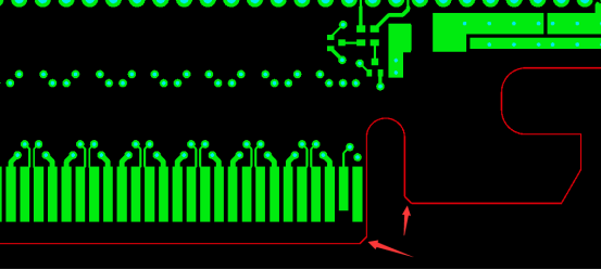
For staggered finger designs, the main lead-out is usually 40 mil and the secondary is 20 mil. When traces enter the board from the connector, use diagonal lines or fillets rather than sharp right angles to improve mechanical and electrical stability.
3. PCB Production Process
The fabrication of a PCB Edge Connector is a high-precision task involving specific plating techniques:
Hard Gold Plating (Electroplated Nickel Gold)
With a thickness of 3-50u", hard gold is used for its superior conductivity, oxidation resistance, and wear resistance. It is the gold standard for interfaces that undergo frequent plugging and unplugging.
ENIG (Electroless Nickel Immersion Gold)
Typically 1-3u" thick, ENIG is used for high-precision boards with BGA or IC bonding. While cost-effective and offering great flatness, it is less wear-resistant than hard gold and is only used for edge connectors that will not be frequently cycled.
[Image comparing Hard Gold vs ENIG surface finishes on a PCB]
4. DFM Testing and Quality Control
Because PCB Edge Connector products are often high-value, manufacturing errors can lead to significant financial loss. Utilizing DFM software before production is essential to:
Verify beveling angles.
Check solder mask windows.
Ensure plating bus bars are correctly positioned.
Pre-production software checks reduce costs and increase production efficiency by catching potential failures before the board reaches the assembly line.
Conclusion
From initial design parameters to the final electroplating stage, every step of creating a PCB Edge Connector requires meticulous attention to detail. By balancing design aesthetics with manufacturing constraints, engineers can ensure their boards provide seamless connectivity and long-term durability.
At PCBGOGO, we offer expert fabrication services for multilayer boards up to 32 layers, specializing in high-reliability PCB Edge Connector production to meet your most demanding signal integrity needs.

