PCB Drilling Design Guidelines: Top 10 Common Issues and Solutions
In the PCB design lifecycle, drilling is a pivotal stage that directly impacts electrical connectivity, assembly quality, manufacturing compatibility, and overall production costs. With the rising demand for high-speed, high-density, multi-layer boards and advanced materials, the tolerance for error in drilling has plummeted. Improper design at the early stages can lead to incorrect hole attributes, opens/shorts, soldering failures, and costly reworks or scrap.
This article summarizes the most frequent drilling errors encountered in mass production and provides actionable PCB Drilling Design Guidelines and DFM (Design for Manufacturing) recommendations to enhance your first-pass yield.
I. Fundamentals of PCB Drilling
Before diving into specific issues, it is essential to define the core drilling types and their attributes:
Why do drilling errors occur? Most issues stem from confusing layer definitions, data loss during E-CAD to CAM conversion, incorrect attribute labeling, and conflicts between solder mask design and annular rings.
II. Common Design Issues & DFM Recommendations
1. Incorrect Hole Attributes
Issue: Conflicting definitions between PTH and NPTH.
Risk: Leads to manufacturing errors where holes are plated when they shouldn't be, or vice versa.
DFM Advice: Design copper annular rings for PTH. For NPTH, ensure no copper pads or traces intersect the hole area.
Pro Tip: Always include a Drill Table with tolerances. PTH usually requires a +0.1mm compensation for plating, while NPTH carries a standard ±0.05mm tolerance.

2. Isolated Holes Defined as PTH
Issue: Holes with no electrical connection are defined as Plated Through Holes in the Gerber or Drill Map.
Risk: Causes confusion for the CAM engineer; may lead to "isolated copper islands" or unnecessary plating.
DFM Advice: Correctly define attributes based on electrical necessity.
3. Missing PTH Status for Component Pads
Issue: Component pads are defined as NPTH despite requiring a solderable connection.
Risk: Total loss of electrical connectivity; parts cannot be soldered to the internal layers.
DFM Advice: Ensure all functional component pads are set to PTH.
4. Overlapping Slots and Round Holes
Issue: A slot and a round hole are placed at the same coordinate, making the intended output ambiguous.
Risk: The round hole might be skipped, or the drill bit may break during the overlapping hit.
DFM Advice: If both are needed, place them clearly in the drill layer. If the round hole is redundant, remove it from the design.
5. Slots Placed in the Drill Map Layer Only
Issue: Slotted holes are only drawn on the Drill Map (legend) layer but not included in the actual NC Drill file.
Risk: High probability of the slots being missed entirely during CNC drilling.
DFM Advice: Always include slot data in the primary NC Drill file or a dedicated mechanical layer.
6. Pad Deformation Due to Proximity
Issue: Component holes are placed too close together. To maintain a solder mask bridge, the pads are "shaved" or clipped.
Risk: Reduced soldering surface area, leading to weak joints or "cold" solder points.
DFM Advice: Increase the hole-to-hole spacing or slightly reduce the finished hole size (if the component lead allows).
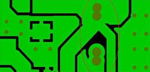
7. Burr Issues in Figure-8 Holes
Issue: Two holes overlap to form an "8" shape.
Risk: Severe copper burrs and "peeling" during drilling, which can cause shorts or plating voids.
DFM Advice: Increase the spacing between the two holes or replace the design with a standard milled slot.

8. Excessive Via Diameter Variance for Solder Mask Plugging
Issue: Vias requiring solder mask plugging have a diameter variance (range) exceeding 0.2mm.
Risk: Difficult to achieve a uniform plug; leads to uneven ink filling and poor protection.
DFM Advice: Keep via sizes consistent. Ensure the difference between the smallest and largest via for plugging is ≤ 0.2 mm.
9. Vias Too Close to Board Edge
Issue: Placing vias too near the routing or V-cut line.
Risk: Exposed copper at the board edge or "broken" hole walls during profiling.
DFM Advice: Maintain a minimum distance of 10 mil between the via wall and the board edge.
10. Drill Conflicts with IC Pads
Issue: Vias are placed directly on or too close to small IC pads.
Risk: Solder wicking (solder stealing), pad fracture, or "pseudo-soldering" (intermittent contact).
DFM Advice: Offset vias from small SMT pads to ensure a reliable solder joint.
III. Summary of DFM Reference Values
To ensure your design is manufacturable, follow these baseline PCB Drilling Design Guidelines:
IV. Conclusion
Mastering drilling design is a cornerstone of PCB Design for Manufacturing (DFM). Errors in hole attributes or placement don't just complicate production—they lead to functional failures, soldering defects, and unnecessary costs. By adhering to these PCB Drilling Design Guidelines, you can ensure your design files are clear, precise, and ready for high-quality fabrication.
PCBGOGO supports advanced drilling requirements down to 0.15mm, offering comprehensive services including via plugging, epoxy filling, and professional DFM reviews to help you achieve a perfect first-pass yield.

