
Optimizing Safety Distance Between High-Frequency PCB Signals and Power Copper
In 5G consumer electronics—such as 5G smartphones, smart routers, and IoT gateways—PCBs must simultaneously handle high-frequency signal transmission and high-voltage power delivery. This creates a major design contradiction:
Too close → high-frequency signal crosstalk increases
Too far → precious PCB area is wasted, hindering miniaturization
Industry data shows that poor spacing between high-frequency signals and power copper in 5G router PCBs leads to >2% signal error rate and 3% power insulation failure rate.
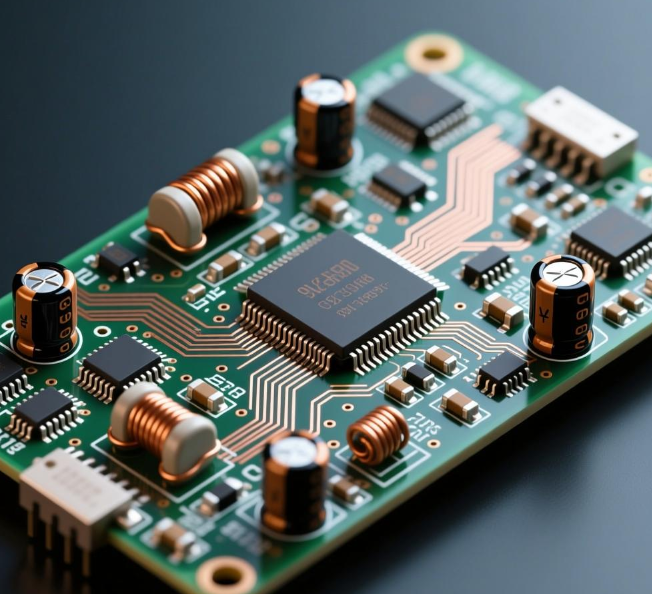
With deep expertise in high-frequency and high-voltage PCB manufacturing, including 12-layer controlled-impedance boards and 5G ENIG PCBs, PCBGOGO provides proven solutions. This blog breaks down the design logic and optimization steps for balancing crosstalk suppression and safe insulation, referencing IPC-2221 and IPC-A-610G standards to help engineers achieve dual compliance.
1. Core Technical Logic: Balancing Safety Distance & Signal Integrity
1.1 Dual Requirements: Signal Integrity vs. Power Insulation
Signal-side requirement: Crosstalk suppression
High-frequency signals (≥2.4GHz) are highly sensitive to electromagnetic coupling.
According to IPC-2221, maintaining a minimum spacing of ≥3W (W = trace width) between a signal trace and a power copper area can reduce crosstalk by ≥40dB.
Power-side requirement: Electrical clearance
Power copper areas must meet electrical safety spacing to avoid insulation breakdown:
12V systems require ≥0.5mm
24V systems require ≥1.0mm
(Reference: IEC 60950-1)
1.2 Why These Requirements Conflict
The conflict arises from limited PCB space.
For example:
A 0.3mm signal trace requires 0.9mm (3W) spacing
A 12V power copper requires 0.5mm spacing
Total requirement: 1.4mm, which is too large for compact consumer electronics.
1.3 PCBGOGO’s Engineering Solution
PCBGOGO applies a dual strategy: shielding isolation + material optimization:
Ground Guard Trace Shielding
0.2mm width, 0.2mm spacing
Acts as an “EM barrier”
Can reduce spacing requirement by up to 30%
High-frequency materials
Rogers RO4350B (Dk = 3.48, Df = 0.0037)
Reduces crosstalk sensitivity
Improves insulation and voltage withstand capability
2. Practical Engineering: Step-by-Step Optimization Guide
2.1 Step 1 — Set Tiered Safety Distance Rules
Based on IPC-2221, IEC 60950-1, and PCBGOGO’s high-frequency PCB standards:
| Signal Frequency | Power Voltage | Recommended Spacing | Primary Goal |
|---|---|---|---|
| ≤2.4GHz | ≤5V | ≥0.5mm | Withstanding voltage |
| 2.4–5GHz | 5–12V | ≥0.8mm | Balance crosstalk & insulation |
| ≥5GHz | ≥12V | ≥1.2mm | Crosstalk suppression |
Key Idea: Do not apply “one-size-fits-all” spacing. Use differentiated spacing based on frequency and voltage.
2.2 Step 2 — Optimize Layout & Routing
Design methods:
Chamfered power copper edges (radius ≥0.5mm) to avoid electric-field concentration
Orthogonal routing between HF signals and power copper (90° angle)
Limit parallel run length ≤30mm
Add ground shield traces between signal and power copper
Width: 0.2mm
Clearance: 0.2mm
Both ends tied to ground (IPC-2221 Sec. 6.4.2)
Tools: Altium Designer 22, PCBGOGO shielding templates.
2.3 Step 3 — Strengthen Shielding & Insulation Technology
Shielding for high-frequency signals
Stainless steel shield case (0.2mm thickness)
Minimum 0.3mm spacing
Ground resistance ≤1Ω
Insulation for power copper
Solder mask thickness ≥15μm
Sunlon halogen-free solder mask (20kV/mm insulation strength)
For extreme tight space: apply local insulation coating
e.g., Dow Corning DC1-2577
Can reduce required spacing by another 20%
2.4 Step 4 — Validate Crosstalk & Withstanding Voltage
Crosstalk Test (Network Analyzer, S-parameters)
NEXT ≤ –45 dB @ 5GHz
FEXT ≤ –50 dB @ 5GHz
Withstanding Voltage Test
1.5× rated voltage for 1 minute (e.g., 12V → 18V test)
No breakdown or leakage >1mA
Meets IPC-A-610G Class 3 requirements
Equipment: Agilent N5230C, Chroma 19073.
Conclusion: Achieving Dual Compliance for High-Frequency & High-Voltage PCB Design
Designing the proper spacing between high-frequency signal traces and power copper areas is fundamentally about tiered balancing, not rigid rules. To ensure both crosstalk suppression and insulation safety, engineers should:
Apply tiered spacing rules based on signal frequency and power voltage
Use shielding techniques such as ground guard traces and metal shield cans
Upgrade materials to low-loss, high-insulation substrates like RO4350B
With advanced manufacturing capabilities in high-frequency, high-voltage, and controlled-impedance PCBs, PCBGOGO helps engineers achieve optimal performance while enabling compact, reliable 5G product designs.

