
OLED PCB Design Guide: Architecture, Manufacturing Process & Applications
OLED displays have redefined what consumers expect from screens: perfect blacks, infinite contrast ratios, ultra-thin profiles, and the flexibility to fold or curve without sacrificing image quality. But the visual performance of every OLED panel begins long before the first pixel lights up — it begins in the design and fabrication of the OLED PCB that controls it. The printed circuit board governing an OLED display must manage precision current delivery to millions of individual pixels, coordinate high-speed data timing, dissipate heat without degrading organic materials, and — in flexible applications — bend thousands of times without failure. This guide examines the engineering requirements, manufacturing processes, board types, and application domains that define modern OLED PCB technology.
What Is an OLED PCB?
An OLED PCB is a printed circuit board specifically designed to drive, control, and power an organic light-emitting diode display. Unlike a standard PCB, which may support a broad range of general-purpose electronic functions, an OLED PCB must satisfy a uniquely demanding set of electrical and physical constraints arising directly from the physics of OLED technology.
OLED pixels are current-driven devices, not voltage-driven. Each sub-pixel emits light in direct proportion to the current flowing through its organic compound — meaning that any variation in current, even at the 1% level, produces visible brightness non-uniformity across the panel. This makes precision current regulation the central engineering challenge of every OLED display PCB design. Additionally, because organic compounds degrade when exposed to heat and moisture, the OLED controller PCB must minimize thermal output, enforce tight thermal boundaries, and often include environmental protection features such as hermetic sealing or conformal coatings.
An OLED PCB is more accurately described as a system of integrated sub-boards and ICs rather than a single component. A complete OLED display PCB assembly typically includes an OLED driver PCB (containing the pixel-level current source ICs), a timing controller board (managing data refresh and image processing), a power management subsystem (generating multiple regulated voltage and current rails), and — in smartphones and wearables — a touch controller integration layer. Together, these form the OLED display PCB ecosystem that turns raw video data into precisely lit pixels.
OLED PCB Architecture: Core Functional Blocks
Understanding how an OLED PCB is organized at the system level is essential for engineers designing or specifying display assemblies. The four primary functional blocks are:
1. OLED Driver PCB — Precision Current Control
The OLED driver PCB is the most electrically critical element of the assembly. It houses the column and row driver ICs that directly interface with the organic light-emitting stack. Each driver IC manages thousands of current sources simultaneously, each calibrated to deliver a precise, individually addressable current to its corresponding sub-pixel. Modern smartphone OLED driver boards achieve ±1% current accuracy across millions of pixels, with real-time compensation algorithms correcting for temperature-induced drift and organic layer aging (which causes luminance to decline over the display's lifetime).
Driver ICs on OLED PCBs are typically packaged as chip-on-film (COF) modules — thin flexible films carrying the driver IC that bond directly to the panel's edge, minimizing the bezel width visible in thin-bezel smartphone designs.
2. OLED Controller PCB — Timing and Image Processing
The OLED controller PCB contains the timing controller (TCON), the central processor managing how pixel data is fed to the driver ICs. The TCON accepts incoming video data (via MIPI DSI in smartphones, or DisplayPort/HDMI in monitors), applies image processing algorithms — including histogram-based brightness enhancement, pixel-level compensation look-up tables, and flicker-reduction PWM schemes — and distributes precisely timed data signals to the driver array. Refresh rates of 60 Hz are standard; flagship smartphone OLED PCBs support 120 Hz or higher, demanding high-speed signal integrity design with controlled impedance traces and careful differential pair routing.
3. Power Management Subsystem
OLED displays require multiple regulated supply rails simultaneously: typically 1.8 V for logic, 3.3 V for interface circuits, 4.5–5 V for the OLED anode, and 12–15 V for the gate drivers — all generated from a single battery or power input. The power management IC (PMIC) on the OLED display PCB handles these conversions using switched-mode power supplies, with ultra-low noise output specifications to prevent switching ripple from appearing as display artifacts. PMIC placement, decoupling capacitor selection, and power plane layout directly affect panel uniformity and EMI emissions.
4. Thermal Management Integration
Organic light-emitting materials degrade faster at elevated temperatures. The OLED PCB must therefore actively manage thermal loads from driver ICs and power management circuits. This is achieved through thermal via arrays connecting component heat sources to internal copper planes, direct copper bonding (DCB) on high-power driver stages, graphite or vapor chamber heat spreaders in premium smartphone OLED assemblies, and thermal interface materials bridging the PCB to the device chassis. Effective thermal design extends the operational lifetime of the organic layer and prevents brightness uniformity degradation over time.
Types of OLED PCB: Rigid vs. Flexible
OLED PCBs are manufactured in two primary form factors — rigid and flexible — each with distinct material stacks, design rules, and application domains. The table below summarizes the key differences:
| Specification | Rigid OLED PCB | Flexible OLED PCB |
|---|---|---|
| PCB Type | Rigid OLED PCB | Flexible OLED PCB |
| Substrate | FR-4 / Rogers (HF) | Polyimide (PI) |
| Min Thickness | 0.4 mm | 0.05–0.2 mm |
| Min Bend Radius | N/A (rigid) | ≥ 1 mm (100k+ cycles) |
| Layer Count | 4–12 layers typical | 2–6 layers typical |
| Trace Width | ≥ 50 μm (HDI: 25 μm) | ≥ 50 μm |
| Surface Finish | ENIG / HASL / OSP | ENIG preferred |
Rigid OLED PCB
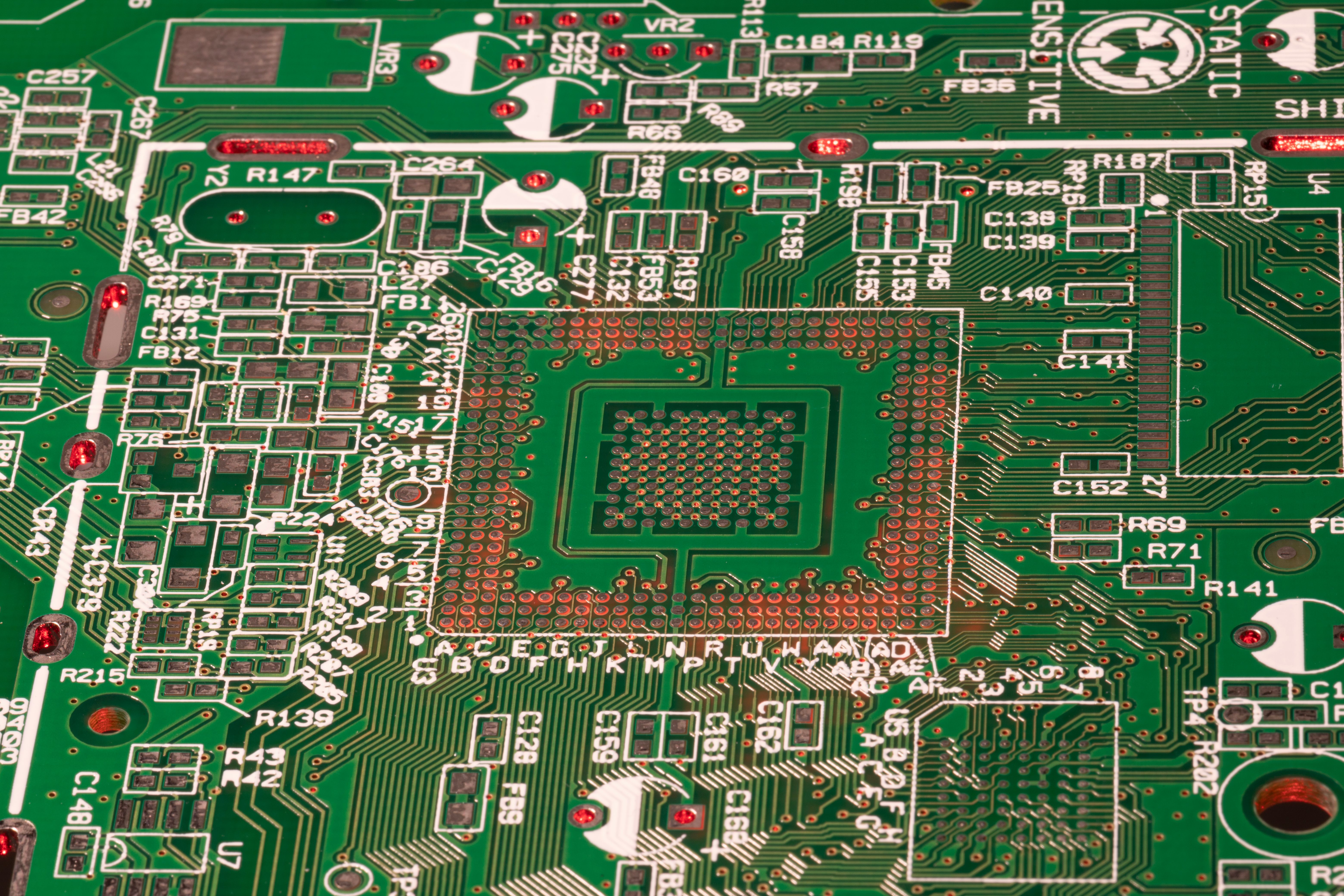
Rigid OLED PCBs use FR-4 fiberglass or high-frequency laminates (such as Rogers 4350B for high-speed signal layers) as their substrate. Layer counts of 4 to 12 are typical in smartphone OLED controller assemblies, with HDI construction — laser-drilled microvias, via-in-pad technology, and sequential lamination — enabling component densities sufficient for fine-pitch BGA and QFN packages at 0.3–0.4 mm pitch. The rigidity of these boards provides mechanical stability for large-area displays in televisions, professional monitors, and medical imaging equipment.
Flexible OLED PCB
Flexible OLED PCBs use polyimide (PI) substrates, which maintain dimensional stability and dielectric performance through repeated bending cycles. In foldable smartphones and wearable devices, the flexible OLED PCB must withstand bend radii as tight as 1 mm for 100,000 or more fold cycles without delamination or conductor fracture. This demands specialized copper foil selection (rolled-annealed copper, which has better ductility than electrodeposited copper), controlled adhesive layer thicknesses, and bend-zone routing rules that avoid placing vias or component pads in areas subject to maximum strain. Flexible PCBs also enable chip-on-film driver mounting, allowing display bezels of 1–2 mm in premium smartphones.
OLED PCB Manufacturing Process
OLED PCB manufacturing follows the standard PCB fabrication sequence but with additional process controls and tighter tolerances demanded by the precision requirements of OLED display systems.
Material Preparation and Laminate Selection
For rigid OLED boards, low-loss FR-4 variants (Tg ≥ 170 °C) or halogen-free materials are selected based on operating temperature and high-speed signal requirements. For flexible boards, polyimide films (25–75 μm thick) with FCCL (flexible copper-clad laminate) serve as the starting material. Material selection directly affects signal integrity at the high data rates used by MIPI DSI and LVDS interfaces in OLED systems.
HDI Layer Build-Up
Most OLED PCB manufacturing uses HDI construction — a sequential lamination process in which core layers are fabricated first, then additional dielectric and copper layers are added with laser-drilled blind microvias connecting adjacent layers. This allows routing of fine-pitch BGA signals that would be impossible in conventional through-hole via designs. Laser drilling accuracies of ±25 μm and via capture pad diameters as small as 150 μm are standard in advanced OLED controller PCB production.
Copper Plating and Trace Formation
Copper traces on OLED driver PCBs carry both high-speed digital signals and sensitive analog current-source outputs. Trace widths on analog current-delivery paths are carefully calculated to maintain voltage drop below specified thresholds across the full current range. Differential pairs carrying MIPI or LVDS data are routed with matched lengths and controlled impedance (typically 85–100 Ω differential), verified by time-domain reflectometry (TDR) during manufacturing.
Surface Finish Selection
Electroless nickel immersion gold (ENIG) is the dominant surface finish for OLED PCBs due to its flat surface profile (critical for fine-pitch BGA soldering), excellent solderability, and compatibility with both SMT assembly and wire bonding where chip-on-board components are used. Immersion silver and OSP (organic solderability preservative) are used in cost-sensitive applications, though ENIG remains the industry standard for OLED display PCB assembly in premium segments.
OLED PCB Assembly
OLED PCB assembly follows SMT best practices with additional requirements: component placement accuracy within ±15 μm for BGA packages, nitrogen atmosphere reflow to minimize oxidation during soldering of sensitive OLED controller ICs, automated optical inspection (AOI) after paste printing and after reflow, and X-ray inspection of all BGA and QFN solder joints. For flexible OLED assemblies, chip-on-film bonding uses anisotropic conductive film (ACF) rather than conventional solder, with thermocompression bonding at 180–200 °C applying pressure and heat to form reliable connections between the COF driver leads and the display panel electrodes.
OLED PCB Applications Across Industries
OLED display technology — and the PCBs that enable it — has expanded well beyond consumer smartphones into a wide range of demanding application sectors.
Smartphone OLED PCB
The smartphone segment represents the highest-volume and most technologically advanced application for OLED PCBs. A flagship smartphone OLED PCB integrates display drivers, touch controllers, fingerprint sensors (in under-display designs), and always-on display logic into an extremely compact multilayer flex and rigid-flex assembly. Foldable smartphones add hinge-crossing flexible circuits that must survive 200,000+ fold cycles while maintaining 120 Hz refresh and HDR color accuracy.
Automotive OLED Displays
Automotive dashboard displays, ambient interior lighting, and advanced instrument clusters increasingly use OLED technology for its wide viewing angles, high contrast, and design flexibility. Automotive OLED PCBs must meet AEC-Q100 qualification standards, operate across ?40 °C to +105 °C junction temperatures, pass vibration and thermal shock testing, and demonstrate EMC compliance with CISPR 25 automotive standards. The OLED controller PCBs used in vehicle applications typically feature conformal coating for moisture protection and redundant power rail monitoring for functional safety.
Wearable and AR/VR OLED Systems
Smartwatches, fitness trackers, and augmented reality headsets use micro-OLED displays — panels as small as 0.5 inch diagonal with pixel densities exceeding 2,000 PPI. The OLED driver PCBs for micro-OLED systems must deliver this resolution within extreme size and power constraints, driving demand for wafer-level chip-scale packaging (WLCSP) and advanced flex PCB construction. VR headsets require high-brightness OLED panels with fast pixel response, demanding driver boards capable of PWM dimming at frequencies above 1 kHz to minimize perceived motion blur.
Medical and Professional Imaging
Surgical monitors, radiology displays, and professional color-critical monitors use OLED panels for their absolute black levels and wide color gamuts, which are clinically significant for tissue differentiation and accurate color rendition. Medical OLED PCBs require compliance with IEC 60601-1 electrical safety standards, FDA and CE marking, and biocompatibility documentation for any surfaces that may contact patients or operating personnel. High-stability current regulation is paramount: brightness uniformity specifications as tight as ±2% across the panel are enforced to prevent misinterpretation of medical images.
Key Design Considerations for OLED PCBs
Engineers designing OLED PCBs for the first time encounter a set of challenges that distinguish OLED systems from conventional display driver designs:
Current matching across pixel arrays: Use precision resistor networks, trimming DACs, or digital compensation tables to achieve <1% current variation across all driver channels.
Power supply noise: Place bulk decoupling capacitors within 1 mm of PMIC output pins; use separate analog and digital ground planes with a single star-point connection to minimize noise coupling from switching regulators to current-source circuits.
Thermal via placement: Place thermal vias under exposed-pad ICs at ≥0.5 mm pitch with 0.3 mm drill diameter; connect to an internal copper plane of ≥2 oz weight to spread heat laterally before it reaches the organic panel stack.
Impedance control for MIPI DSI: Route differential pairs as edge-coupled microstrips or striplines at 85–100 Ω; maintain ≤5 mm length mismatch within each pair and ≤20 mm skew between pairs in the same lane group.
Bend zone rules (flex designs): Keep all traces parallel to the bend axis in the flex zone; avoid vias within 2 mm of the bend centerline; minimize copper weight in the bend zone to 0.5 oz to reduce strain concentration.
Moisture protection: Apply IPC Class SIR-compliant no-clean flux in assembly and conformal coat automotive and outdoor OLED PCBs with acrylic or polyurethane coatings to a minimum 25 μm cured thickness.
Conclusion
The OLED PCB is the invisible engineering foundation beneath every high-quality OLED display. Whether it is the ultra-thin flexible OLED PCB folding inside a smartphone, the thermally robust OLED controller PCB driving an automotive instrument cluster, or the precision micro-OLED driver PCB enabling augmented reality, the performance of the PCB defines the performance of the display. Success in OLED PCB design requires mastery of precision analog current control, high-speed digital signal integrity, advanced multilayer HDI fabrication, and — in flexible applications — the mechanical reliability engineering that keeps bending circuits alive across hundreds of thousands of cycles.
As OLED technology continues to expand into new form factors — foldable, rollable, transparent, and micro-OLED — the demands placed on OLED PCB manufacturing will only intensify. Engineers who understand the unique electrical, thermal, and mechanical requirements of OLED display PCB design will be best positioned to bring the next generation of display technology to market.


