
Mobile HDI PCB Blind & Buried Via Process Optimization: Improving Yield and Reliability
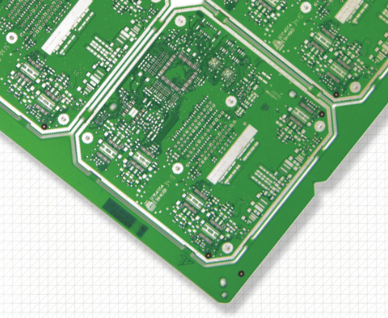
As smartphones move toward lighter, thinner bodies and multi-camera architectures, HDI PCBs have become the backbone of mobile electronics. With line width/spacing ≤ 0.1 mm and blind/buried via diameters ≤ 0.2 mm, HDI boards require extremely precise micro-via fabrication.
However, the blind & buried via process is the main determinant of HDI yield. Industry data shows that without process optimization, void rates can exceed 8%, pushing mainboard rework rates above 12%. One smartphone brand even scrapped 5,000 PCBs in a single day due to plating voids—causing over $30,000 in direct losses.
PCBGOGO has specialized in mobile HDI board manufacturing for 8+ years and delivered 20 million+ mobile HDI PCBs, achieving 99%+ blind via yield stability. This article breaks down the core process challenges, critical parameters, and best-practice quality control to help consumer electronics manufacturers achieve high-volume, high-reliability HDI production.
Understanding Blind & Buried Via Challenges in Mobile HDI PCBs
HDI blind/buried via fabrication must strictly follow IPC-6012 Section 3.6 for micro-via qualification. The core challenge is achieving perfect via wall quality in extremely small diameters.
1. Drilling Accuracy
Typical blind via diameter: 0.15–0.2 mm
Position deviation requirement: ≤ ±0.02 mm
Deviation above ±0.03 mm increases the open-circuit rate by 15%
(Defined in IPC-2226 Section 4.2)
2. Via Wall Roughness
Required roughness: ≤ 1.5 μm
Roughness >2 μm increases plating void rate by 20%
Tested per IPC-TM-650 2.2.17
3. Copper Plating Thickness
Via wall copper thickness: ≥ 18 μm
Uniformity tolerance: ±2 μm
Copper thickness <15 μm increases signal loss by 8%
(According to GB/T 4677 Section 5.3)
Recommended HDI base material:
Shengyi S1130 (Dk 4.3±0.2, thickness 0.1–0.3 mm) — ideal resin flow for via filling.
For drilling, PCBGOGO uses FANUC CNC micro-drilling machines (precision ±0.005 mm). For plating, an acid copper system ensures excellent copper uniformity.
Four-Step Blind & Buried Via Process Optimization
Below is the complete optimization process used in PCBGOGO’s HDI production lines.
Step 1: Drilling Parameter Optimization
Via diameter: 0.2 mm
Spindle speed: 180,000 rpm
Feed rate: 50 mm/min
Retract speed: 80 mm/min
PCBGOGO testing shows:
When spindle speed rises above 200,000 rpm, via wall carbonization reaches 12%.
Equipment: FANUC DR-300
Inspection: Optical microscope spot-check 10 panels per hour.
Step 2: Via Wall Pre-Treatment (Desmear + Micro-Etching)
Desmear temperature: 80°C ± 2°C, time: 6 min
Micro-etching amount: 1.5–2 μm
Ensures via wall roughness ≤ 1.5 μm
Equipment: JPE-Desmear-600
Standard: IPC-TM-650 2.3.11
Step 3: Electroplating Parameter Optimization
Acid copper plating
Current density: 1.8 A/dm2
Temperature: 25°C ± 1°C
Agitation: 300 rpm
Time: 25 min
Ensures:
Copper thickness ≥ 18 μm
Uniformity ≤ ±2 μm
Inspection: 50 panels per batch using JPE-Cu-500 copper thickness tester.
Step 4: Via Filling & Curing
Filling material: Epoxy resin (viscosity 5000 cP @25°C)
Curing temperature: 150°C ± 5°C, time: 40 min
Filling completeness: ≥ 98% (IPC-A-600G Class 2 requirement)
Inspection: X-Ray (JPE-XR-900)
Requirement: Via void rate ≤ 0.5%
Mass Production Quality Control Strategy
1. First-Article Verification (FAI)
Via position deviation ≤ ±0.02 mm
Via copper thickness ≥ 18 μm
Void rate ≤ 0.5%
Only approved lots can enter mass production.
2. In-Process Monitoring
Every 2 hours:
Sample size: 20 panels
Monitor:
Plating current deviation: ≤ ±0.1 A/dm2
Filling temperature deviation: ≤ ±2°C
Triggered automatically by PCBGOGO’s Process Early-Warning System when abnormalities appear.
3. Final Inspection
Void rate ≤ 0.8%
Via copper thickness ≥ 18 μm
Position deviation ≤ ±0.02 mm
Batch pass rate ≥ 99%
Failures are analyzed by PCBGOGO’s HDI defect analysis team, which provides a root-cause report and corrective action.
Conclusion
Optimizing blind & buried vias in mobile HDI PCBs requires precise control over four key factors:
Drilling accuracy → Via wall preparation → Copper plating uniformity → Resin filling completeness
PCBGOGO provides a full-process HDI manufacturing solution, including:
DFM analysis with JPE-DFM 7.0
FANUC micro-drilling + automated plating lines
Complete X-Ray inspection of via quality
99%+ stable mass-production yield
This closed-loop approach—spanning design, manufacturing, and quality assurance—ensures mobile device manufacturers can scale HDI production with high reliability and minimal defect rates.

