
Mixed-Technology PCB Assembly: How to Combine Reflow and Wave Soldering
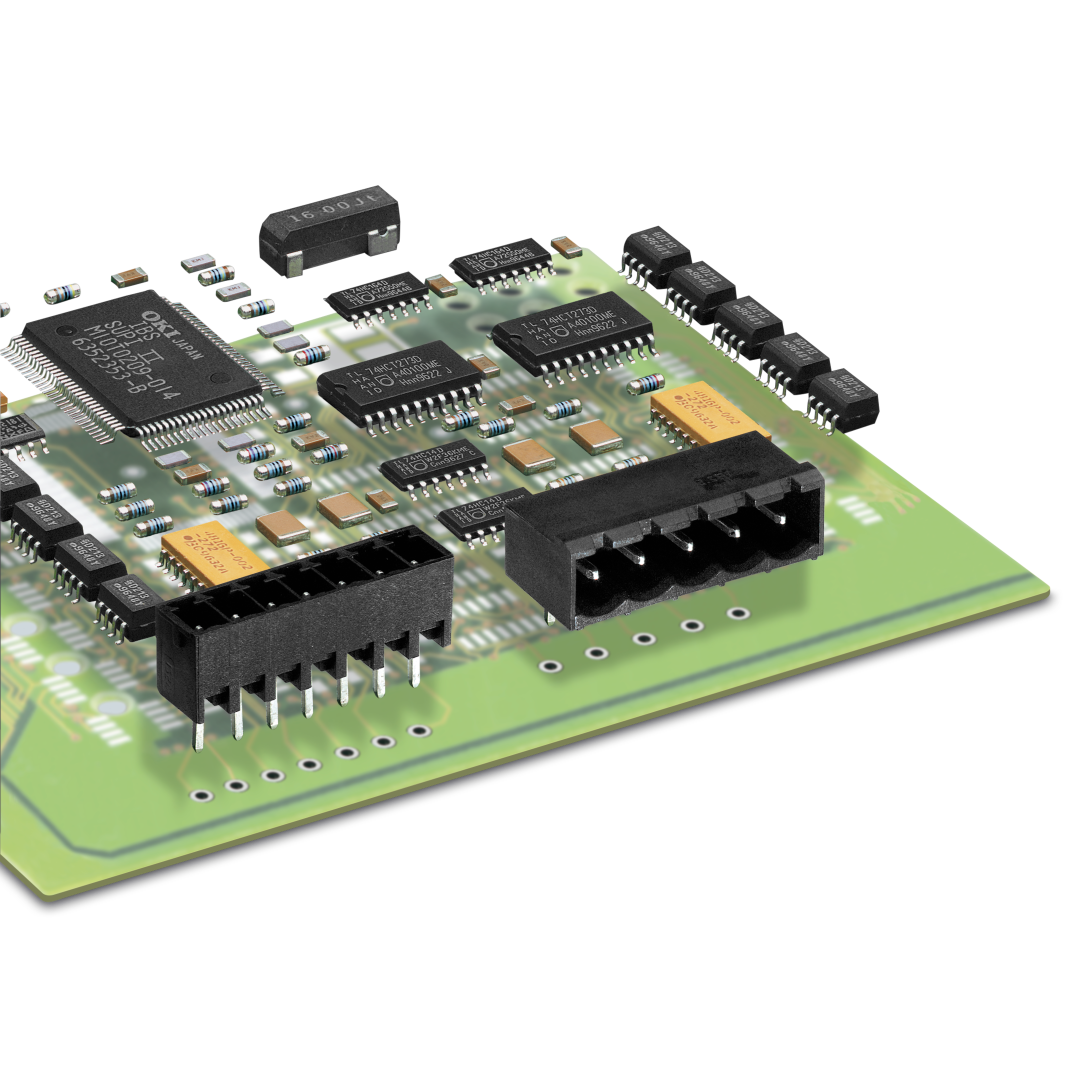
As electronic products become smaller, more powerful, and more complex, PCB designers increasingly rely on mixed-technology PCB assembly, where surface-mount technology (SMT) and through-hole technology (THT) coexist on a single board. This hybrid approach enables high-density placement of miniature components while preserving the mechanical strength and reliability needed for large connectors, power devices, and mission-critical circuitry.
To assemble such boards efficiently, manufacturers must combine reflow soldering for surface-mount components with wave soldering (or selective soldering) for through-hole components. This article provides a comprehensive guide on how the two processes integrate, best practices for optimizing manufacturability, and design considerations to achieve high solder quality and yield.
What Is Mixed-Technology PCB Assembly?
Mixed-technology assembly refers to PCB designs that incorporate both SMD and THT components. SMT components are soldered using reflow soldering, while THT components typically require wave soldering or selective soldering.
Typical Industries Using Mixed Technology
Automotive electronics (ECUs, ADAS modules)
Power supply and power converter boards
Industrial automation controllers
Telecom and networking equipment
Consumer electronics
Medical and aerospace electronics
These sectors often require:
High component density (SMD)
Robust mechanical joints for connectors, coils, and high-current components (THT)
Cost-efficient high-volume production
Why Combine Reflow and Wave Soldering?
Each method excels in specific areas, allowing manufacturers to optimize performance, cost, and reliability.
Advantages of Reflow Soldering (SMT)
Supports extremely small components: 0201, 01005, BGAs, QFNs
Precision-controlled solder joints
Compatibility with double-sided SMT assembly
Reduced thermal shock
Ideal for high-density multilayer PCBs
Advantages of Wave Soldering (THT)
Fast, cost-effective soldering for large quantities
Extremely strong joints due to complete hole-fill
Reliable for connectors and heavy components
Excellent wetting performance for plated through-holes
Combining the two creates a workflow optimized for speed, cost, mechanical strength, and miniaturization—a core requirement in modern electronics.
How Mixed-Technology PCB Assembly Works
1. SMT Assembly and Reflow Soldering
This is always the first soldering step because reflow soldering requires solder paste, which cannot withstand wave solder temperatures afterward.
SMT Reflow Process
Solder paste printing using laser-cut stainless steel stencils
Pick-and-place placement of SMD components
Reflow soldering using a controlled temperature profile
Cooling to solidify joints
For double-sided SMT:
Side A is reflowed first
Side B may require adhesive gluing, low-melt solder paste, or optimized pad design
Bottom-side components must withstand later exposure to wave soldering or be shielded
Related keywords included: reflow soldering temperature profile, SMT assembly process, double-sided reflow.
2. THT Component Insertion
After SMT assembly, operators or automated insertion machines mount THT components such as:
High-current connectors
Transformers, inductors, relays
Large electrolytic capacitors
Wire-to-board terminals
Mechanical switches
Pins are prepared for wave soldering by trimming leads to suitable length and ensuring proper vertical alignment.
3. Wave Soldering of THT Components
Wave soldering is the main technique used for mixed-technology THT soldering unless layout density requires selective soldering.
Wave Soldering Process Steps
Fluxing – spray or foam flux to clean oxides and improve solder wetting
Preheating – reduce thermal shock and activate flux
Solder wave contact – PCB passes over a wave of molten solder
Cooling – solder joints solidify under controlled conditions
Key Wave Soldering Parameters
Conveyor speed
Wave height and wave angle
Solder pot temperature (typically 245–265°C for lead-free)
Flux density and flux deposition
Preheat temperature profile
Dwell time
Related keywords included: wave soldering process steps, wave soldering temperature, solder wave height, flux application, PCB wave soldering settings.
Critical Design Guidelines for Mixed-Technology PCBs
Successful integration of reflow and wave soldering requires specific layout strategies:
1. Bottom-Side Component Clearance
Bottom-side SMT parts must either be:
Wave-solderable (chip resistors, SOT-223, small SMDs), or
Mask-shielded using wave pallets/fixtures to prevent solder contact
2. Correct THT Hole-to-Lead Ratios
Proper barrel fill depends on:
Lead diameter
Hole diameter
Copper plating thickness
Thermal relief pad design
3. Solder Thieves and Anti-Bridging Techniques
For connectors or fine-pitch THT pins, solder thieves help prevent bridging during wave soldering.
4. Thermal Relief Pads
Large copper pours must use thermal relief spokes to ensure:
Adequate heat transfer
Proper solder wetting
Reduced tombstoning for nearby SMT parts
5. Component Orientation for Wave Flow
Align THT solder pads and SMT pads parallel to solder wave direction to reduce:
Bridging
Shadowing
Icicle formation
Related keywords included: wave soldering defects, solder bridging prevention, barrel fill optimization, PCB layout for wave soldering.
Common Challenges in Mixed-Technology Assembly
Mixed-technology assembly must be carefully managed:
SMT component detachment during wave soldering
Excessive temperature causes warpage
Shadowing leading to incomplete solder joints
Lead-free wave soldering bridges
Inconsistent flux activation
THT pins blocking wave flow
A capable manufacturer must optimize process parameters and fixtures to maintain high yield.
Conclusion
Mixed-technology PCB assembly leverages the strengths of reflow soldering and wave soldering to produce compact, reliable, and high-performance electronics. By carefully coordinating these two soldering methods—along with optimized PCB layout, and precise process control—manufacturers can achieve high yields even for complex and densely populated PCB designs.
If you want your next project assembled with precision, consistency, and industry-level expertise, PCBGOGO has the capability and experience to support your entire manufacturing process from PCB fabrication to complete PCBA assembly.

