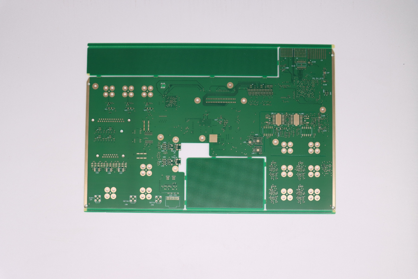
Minimizing Vias The Key to High-Density PCB Design
The trend in electronics is clear: everything must be smaller, faster, and more powerful. For us in the PCB industry, this relentless push means constantly shrinking one critical feature: the minimum hole size (or smallest via). This little hole is perhaps the biggest factor limiting how dense your circuit board can be.
Why Minimum Hole Size Matters: Density and Drill Limits
Minimum hole size directly dictates a board's circuit density because smaller vias take up less valuable real estate. But going too small creates significant manufacturing challenges, mainly impacting drilling and plating reliability.
1. The Impact on Drilling and Density
Higher Density Routing: When vias are small, their surrounding copper pads (annular rings) can also be smaller. This frees up space between pads, allowing designers to route more traces (wires) through a tight area—especially crucial for complex components like BGAs (Ball Grid Arrays).
Drilling Technology: The smallest through-holes are made using high-speed mechanical drills, which are prone to wear and breakage when drilling extremely small diameters, especially through thick material. The smallest commercially reliable hole size for standard drilling is typically 0.15mm to 0.20mm.
Laser Drilling (Microvias): To achieve higher density (like in HDI PCBs), manufacturers use laser drilling to create microvias (often ≤0.1mm diameter). These vias connect only one or two layers at a time, bypassing the thickness constraint of traditional drilling.
2. The Critical Aspect Ratio Challenge
The biggest reliability constraint is the Aspect Ratio (AR), defined as the ratio of the board's thickness to the drilled hole's diameter:
Aspect Ratio=Drill DiameterBoard Thickness
Plating Reliability: A high AR (e.g., 10:1 or higher) means a deep, narrow hole. During the copper plating process, the chemical solution struggles to uniformly deposit copper deep inside these narrow holes. Thin copper in the middle of the via wall can lead to failure (cracking) when the board undergoes thermal stress (like during soldering or operation).
Practical Limit: For standard through-hole vias, the industry generally adheres to an AR limit of 8:1 to 10:1 to ensure robust copper plating. For microvias, the AR must be extremely low, typically ≤1:1.

Practical Design Considerations (Reference Guide)
To balance performance and manufacturability, follow these guidelines when pushing the limits of hole size:
| Design Feature | Goal | Typical Reference Value (Via) |
| Minimum Finished Hole | Use for PTH/Vias, not components | 0.20mm (≈8mil) for standard density |
| Microvia Diameter | Required for HDI/BGA escape routing | ≤0.10mm (≈4mil) |
| Annular Ring (Min.) | Ensure reliable connection after drill tolerance | ≥0.05mm (≈2mil) |
| Aspect Ratio (Max.) | Guarantee uniform copper plating | 8:1 to 10:1 (Through-Hole) |
Modern Trend: The use of Via-in-Pad (VIP) technology, where small vias are placed directly on the component pad and then filled/capped, is common in high-density designs (like smartphone mainboards) to save space and improve signal paths.
The Future: Miniaturization and Manufacturing
The demand for high-performance computing, 5G devices, and automotive radar is driving miniaturization further. This means more HDI boards, more microvias, and tighter tolerances. The future of PCB fabrication lies in mastering these sub-0.1mm drilling and plating processes.
At PCBgogo, we recognize that achieving the smallest, most reliable vias requires specialized equipment and stringent process control. We have invested heavily in laser drilling technology and advanced plating chemistry to reliably manufacture boards with high aspect ratios and microvia structures, ensuring that your cutting-edge designs meet Class 2 and Class 3 reliability standards. Our commitment is to push our minimum capabilities so you can push your design limits.

