Layer by Layer: Crafting Multilayer PCBs for Enhanced Performance Through-Hole PCB Prototype-PCBGOGO
In today's rapidly advancing technological landscape, the demand for efficient, high-performance electronic devices is ever-growing. At the heart of these devices lie printed circuit boards (PCBs), the backbone of modern electronics. Among various PCB types, multilayer PCBs are gaining prominence for their ability to enhance performance, especially in complex electronic systems. This article explores the intricacies of crafting multilayer PCBs, emphasizing through-hole PCB prototypes and how PCBGOGO excels in this domain.
What Are Multilayer PCBs?
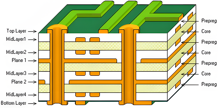
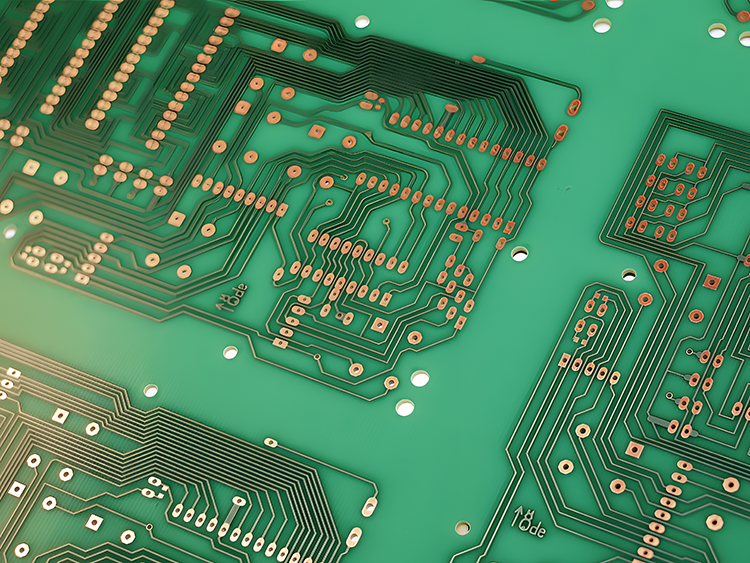
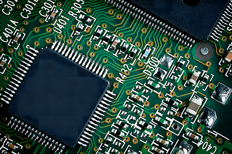
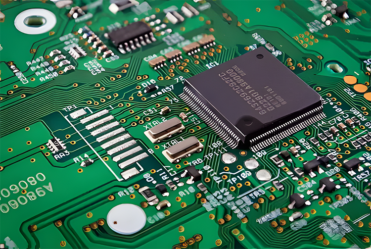
Multilayer PCBs consist of multiple layers of conductive material, usually copper, sandwiched between insulating layers. These boards typically have three or more conductive layers, with two outer layers and one or more inner layers. The construction of multilayer PCBs allows for more complex designs, higher component density, and improved electrical performance, making them ideal for sophisticated applications such as aerospace, telecommunications, and advanced consumer electronics.
Compared to single-layer and double-sided PCBs, multilayer PCBs are constructed with three or more conductive layers. These layers are interconnected through plated through-holes, ensuring electrical connections across the board. Multilayer PCBs can vary in complexity, ranging from 4 to over 100 layers, providing more copper conductive layers and increased wiring space. This design enhances signal transmission and electrical performance, making multilayer PCBs ideal for complex applications.
The manufacturing process for multilayer PCBs is more intricate than that of single-layer or double-sided boards, requiring careful attention to detail. Electrical connections between layers are achieved using plated through-holes, as well as buried or blind vias, ensuring optimal functionality in advanced electronic systems.
The Need for Multilayer PCBs in Modern Electronics
With the increasing complexity of electronic devices, single and double-layer PCBs often fall short of meeting the performance requirements.

Multilayer PCBs offer several advantages over their simpler counterparts:
Enhanced Signal Integrity: The presence of multiple layers allows for better control of signal pathways, reducing noise, crosstalk, and electromagnetic interference (EMI). This is particularly important in high-speed and high-frequency applications.
Higher Component Density: Multilayer PCBs provide more real estate for components, enabling more compact and powerful designs. This is crucial for modern devices where space is at a premium.
Improved Thermal Management: The layered structure facilitates better heat dissipation, which is essential for maintaining the reliability and longevity of electronic components.
Reduced Interconnections: By incorporating multiple layers, designers can reduce the number of interconnections between components, leading to faster signal transmission and increased reliability.
Crafting Multilayer PCBs: The Manufacturing Process
The process of manufacturing multilayer PCBs involves several critical steps, each requiring precision and expertise to ensure optimal performance. Here's a step-by-step breakdown:
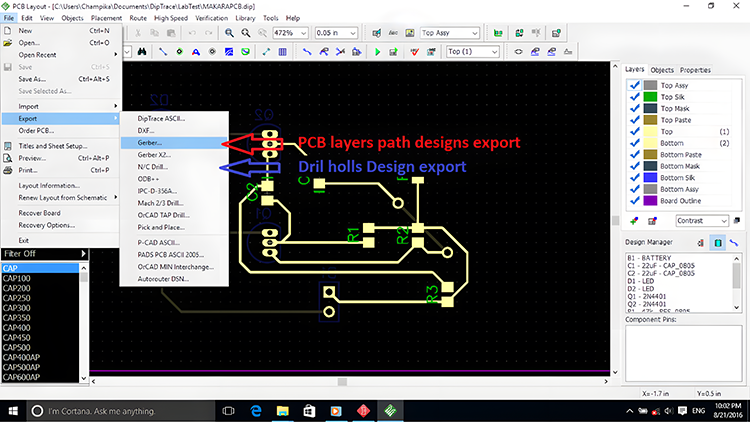
1. Designing the PCB Layout: The first step is to create a detailed PCB layout using specialized software like Altium Designer or Eagle. This layout includes the placement of components, routing of signal traces, and the arrangement of layers. Designers must carefully plan the stack-up of layers to balance performance and manufacturability.
2. Fabricating the Core Layers: The core layers of the PCB are fabricated by laminating copper foil onto a dielectric substrate, typically made of materials like FR4 or Rogers. These core layers form the foundation of the PCB and determine its mechanical and electrical properties.
3. Aligning and Laminating the Layers: The core layers are carefully aligned and laminated using heat and pressure. This step requires precise alignment to ensure that the vias (holes connecting different layers) are correctly positioned. Misalignment can lead to faulty connections and compromised performance.
4. Drilling and Plating Through-Holes: Once the layers are laminated, holes are drilled through the PCB to create pathways for electrical connections between layers. These through-holes are then plated with copper to ensure reliable conductivity. Through-hole technology is particularly advantageous in prototypes as it provides robust mechanical connections and is easier to inspect.
5. Etching the Copper Layers: The copper layers are etched to create the desired circuit patterns after drilling and plating. This involves applying a resist material to protect specific areas of copper while the unprotected areas are removed through a chemical etching process.
6. Applying Solder Mask and Silkscreen: A solder mask is applied to protect the copper traces and prevent solder bridges during assembly. A silkscreen layer is also added, which contains labels, logos, and other markings to aid in component placement and identification.
7. Testing and Quality Control: Before assembly, the PCB undergoes rigorous testing to ensure that it meets the required specifications. This includes electrical testing, visual inspection, and automated optical inspection (AOI) to detect any defects or anomalies.
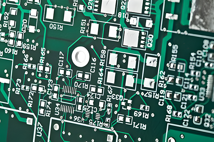
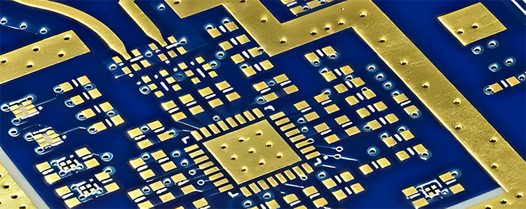
Structure of Multilayer PCB Boards
Multilayer PCBs consist of several essential components that contribute to their functionality and durability. Understanding each element's role is crucial for optimizing PCB design and performance.
1. Dielectric/Substrate:
The dielectric material, often referred to as the substrate, serves as the insulating layer between the conductive layers. It provides mechanical support and maintains electrical insulation between circuits. Common dielectric materials include FR4, which offers a balance of performance and cost-effectiveness, as well as advanced materials like Rogers for high-frequency applications.
2. Through-Hole/Vias:
Vias are critical for establishing electrical connections between different layers of the PCB. There are several types of vias:
· Through-Holes: These extend through the entire board, connecting all layers. Larger through-holes are used for mounting components.
· Buried Vias: These connect internal layers without reaching the outer layers, ideal for compact designs.
· Blind Vias: These connect an external layer to one or more internal layers without passing through the entire board.
· Non-Plated Through-Holes (NPTH): These are used for mounting and positioning components during assembly, particularly for surface-mount devices and fixing screws.
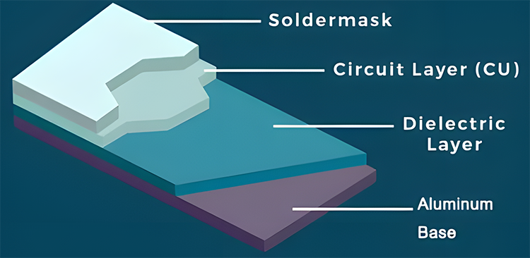
3. Solder Mask:
The solder mask, commonly referred to as solder resist, protects the PCB's copper traces from oxidation and prevents solder bridges during assembly. It comes in various colors, with green, red, and blue being the most popular. The choice of color can depend on both aesthetic preferences and process requirements.
4. Silkscreen/Legend:
The silkscreen layer, while not essential, plays a crucial role in identifying components and guiding assembly. It provides printed information on the board, such as part numbers, logos, and reference designators, facilitating maintenance and troubleshooting.

5. Surface Finish:
To protect the exposed copper on the PCB and ensure good solderability, various surface finishes are applied. These finishes prevent oxidation and improve the board's lifespan. Common surface treatment options include:
· HASL (Hot Air Solder Leveling): A cost-effective and widely used method, that offers good solderability. Hot air solder leveling (HASL) has long been a popular surface finish choice for PCBs, thanks to its affordability and availability. It provides an excellent solderable surface, making it a preferred option for many manufacturers over the years.
However, with the introduction of the RoHS (Restriction of Hazardous Substances) directive, there has been a significant shift from traditional HASL to lead-free HASL.
This transition aligns with global environmental standards, ensuring that the PCB manufacturing process is safer and more sustainable while still maintaining the reliable solderability that HASL is known for.
· Lead-free HASL: While lead-free HASL remains cost-effective, it also supports modern requirements for eco-friendly electronics production. This shift doesn't just meet regulatory demands; it also enhances the marketability of the final products, as more consumers and industries prioritize green manufacturing practices.
· ENIG (Electroless Nickel Immersion Gold): Provides a flat surface, is excellent for fine-pitch components, and offers good corrosion resistance. Electroless nickel immersion gold (ENIG) is a metallic finish applied to printed circuit boards and ceramic substrates that provides a flat, solderable surface. This finish protects the underlying copper from oxidation, ensuring both solderability and compatibility with aluminum wire bonding.
· Applications:
1. Suitable for printed circuit boards and substrates used in SMD (Surface-Mount Device), CoB (Chip on Board), and HDI (High-Density Interconnect) technologies.
2. Ideal for PCBs requiring both soldering and aluminum wire bonding.
3. Serves as a reliable contact surface for keypads and other input devices.
· Advantages:
1. Provides a reliable surface finish on printed circuit boards for soldering and aluminum wire bonding.
2. Ensures high solder joint reliability with both lead-free and leaded soldering processes.
3. Delivers excellent contact surfaces, ideal for various applications.
4. Electroless nickel deposition offers superior edge coverage and supports fine-line designs.
5. More cost-effective compared to electrolytic gold layer finishes.
· Immersion Gold/Silver/Tin: These finishes offer different levels of performance based on cost, solderability, and application needs.
· OSP (Organic Solderability Preservative): A lead-free, environmentally friendly option that provides a thin protective layer for the copper. Organic Solderability Preservative (OSP) is a coating method used on printed circuit boards, where a water-based organic compound is applied.
This compound selectively adheres to the copper surfaces, protecting the soldering process. Common compounds used in OSP coatings belong to the azole family, including benzotriazoles, imidazoles, and benzimidazoles.
Each surface finish has its advantages and trade-offs, so selecting the appropriate finish depends on the specific requirements of the PCB, including its application, budget, and assembly process.
By understanding the structure of multilayer PCBs and the role each component plays, designers can optimize their boards for better performance, reliability, and manufacturability. Whether you're dealing with simple electronics or complex, high-density applications, these elements are fundamental to creating a robust and efficient PCB.
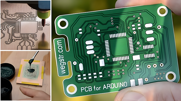
Through-Hole PCB Prototypes: A Vital Step in Development
Through-hole technology, though considered older compared to surface-mount technology (SMT), remains a pivotal aspect of PCB prototyping. Components are mounted by inserting leads through holes in the PCB and soldered to pads on the opposite side, providing significant advantages during the prototyping phase.
Key Advantages of Through-Hole PCB Prototypes:
1. Mechanical Strength:
Through-hole components are mechanically more robust, making them ideal for prototypes that require testing under harsh conditions or need to be mounted on rugged equipment.
2. Ease of Testing:
Through-hole connections are easier to inspect visually, making the prototyping process more straightforward. This is particularly beneficial during the initial stages of development when frequent testing and modifications are needed.
3. Durability and Strength:
Through-hole components are known for their strong mechanical bonds. This makes them highly resistant to physical stress and vibrations, making through-hole PCB prototypes ideal for testing in harsh environments or applications that require robust components.
4. Ease of Manual Assembly:
During the prototyping phase, engineers and developers often prefer through-hole technology due to its ease of manual assembly and soldering. This allows for quick modifications, repairs, and testing, which are essential during early development stages.
5. Reliable Connections:
Through-hole PCBs ensure secure and reliable electrical connections, as components are soldered on both sides of the board. This is particularly important in high-power applications, where stable connections are critical to the performance of the prototype.
6. Flexibility for Testing and Debugging:
Through-hole PCB prototypes allow for easier testing and debugging compared to surface-mount technology (SMT). Components can be easily removed, replaced, or re-soldered, facilitating iterative testing and refinement during development.
7. Compatibility with Breadboarding:
Prototyping often involves breadboarding for circuit testing and design validation. Through-hole components are compatible with breadboards, making it easier to transition from breadboarding to PCB prototyping and ensuring consistency in design. Through-hole components can be easily used with breadboards, enabling rapid prototyping and testing of circuit designs.
8. Thermal Performance:
Through-hole components tend to have better heat dissipation compared to their surface-mount counterparts. This can be advantageous in prototypes that are subjected to higher power loads or require improved thermal management.
Applications of Multilayer PCBs Using Through-Hole Technology
Multilayer PCBs, especially when integrated with through-hole technology, have a broad range of applications across various industries. Through-hole technology, known for its durability and reliability, is often preferred in environments requiring high mechanical strength and enhanced performance. Below are some additional applications where multilayer PCBs with through-hole technology play a crucial role:
1. Aerospace and Defense:
In aerospace and military applications, reliability and durability are paramount. Multilayer PCBs with through-hole components are used in avionics systems, radar, communication devices, and missile guidance systems. The robust nature of through-hole technology ensures that these critical components can withstand extreme conditions, including high temperatures, vibrations, and mechanical stress.
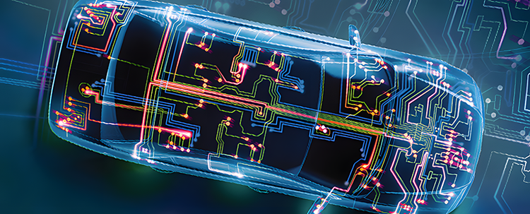
2. Automotive Electronics:
The automotive industry increasingly relies on multilayer PCBs with through-hole technology for systems like engine control units (ECUs), anti-lock braking systems (ABS), and advanced driver-assistance systems (ADAS). These PCBs provide the necessary reliability and durability required in high-temperature and high-vibration environments, ensuring vehicle safety and performance.
3. Medical Devices:
In medical technology, where precision and reliability are essential, multilayer PCBs with through-hole components are used in life-saving equipment such as pacemakers, imaging systems, and diagnostic devices. These PCBs provide the stable electrical connections needed for consistent performance, even in critical applications.

4. Renewable Energy Systems:
Multilayer PCBs with through-hole technology are also pivotal in renewable energy solutions, including solar inverters, wind turbine controls, and energy storage systems. These PCBs ensure that the systems can handle high power levels and operate efficiently over long periods, contributing to the reliability of sustainable energy sources.
5. Industrial Power Supplies:
In industrial applications, power supply units (PSUs) require stable performance under high loads. Multilayer PCBs with through-hole components are used in PSUs for industrial machinery, data centers, and telecommunications infrastructure, providing the necessary power handling capabilities and ensuring long-term reliability.
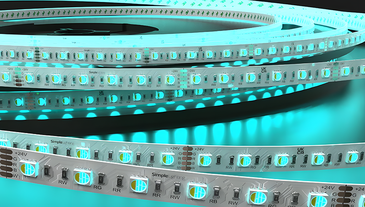
6. LED Lighting Systems:
LED technology is widely used in automotive, architectural, and consumer electronics applications. Multilayer PCBs with through-hole technology enhance the durability and thermal management of LED circuits, ensuring consistent performance and longevity of lighting systems.
7. Consumer Electronics:
In devices like gaming consoles, high-end audio equipment, and advanced home appliances, multilayer PCBs with through-hole components offer enhanced durability and performance. The combination of multilayer design and through-hole technology allows these devices to handle complex functionalities and high electrical loads.
8. Power Amplifiers:
In RF and audio applications, power amplifiers require high-performance PCBs to ensure signal clarity and power efficiency. Multilayer PCBs with through-hole technology provide the necessary electrical and mechanical strength to handle high-frequency signals and power demands.
Through-hole technology, combined with the versatility of multilayer PCBs, continues to support advancements in various industries by offering reliable, high-performance solutions. As technology progresses, these PCBs will only expand, further solidifying their role in critical applications where performance and durability are non-negotiable.
PCBGOGO: Your Partner in Multilayer PCB Prototyping
When it comes to crafting high-quality multilayer PCBs, PCBGOGO stands out as a trusted partner. With state-of-the-art manufacturing facilities and a commitment to quality, PCBGOGO offers a range of services tailored to meet the needs of engineers and designers:
Custom Multilayer PCB Manufacturing: PCBGOGO provides custom multilayer PCB manufacturing services, catering to various industries and applications. Their advanced fabrication techniques ensure precision and reliability in every board they produce.
Quick Turnaround Times: In the fast-paced world of electronics, time is of the essence. PCBGOGO offers quick turnaround times, ensuring that your prototypes are ready when you need them.
High-Quality Standards: PCBGOGO adheres to stringent quality control measures, including ISO and UL certifications. This ensures that every PCB meets the highest standards of performance and reliability.
Affordable Pricing: Despite offering top-notch services, PCBGOGO maintains competitive pricing, making high-quality multilayer PCBs accessible to businesses of all sizes.
Expert Support: PCBGOGO's team of experienced engineers is available to provide guidance and support throughout the entire PCB prototyping process, from design to assembly.
Conclusion
The demand for multilayer PCBs is on the rise as electronic devices become more complex and compact. Through-hole PCB prototyping remains a vital step in the development process, offering mechanical robustness and ease of testing. With a reliable partner like PCBGOGO, engineers, and designers can confidently craft high-performance multilayer PCBs that meet the demands of modern technology.
Whether you're working on a cutting-edge telecommunications device or a sophisticated aerospace system, multilayer PCBs are essential for achieving the performance and reliability your project requires. Trust PCBGOGO to bring your designs to life, layer by layer


