Key Considerations for Designing PCB Prototypes: Tips for Manufacturers and Assemblers
In the fast-evolving world of electronics, printed circuit boards (PCBs) form the backbone of innovation. Whether it's a state-of-the-art medical device or a next-generation IoT gadget, PCB prototypes are essential in turning ideas into functional products. The path to a flawless PCB prototype, however, requires meticulous planning, collaboration, and execution.

This article will guide PCB manufacturers and assemblers through the critical considerations to optimize the design, manufacturing, and assembly processes. With insights tailored for professionals, these tips will ensure high-quality, cost-effective, and efficient PCB prototypes. These prototypes are used to validate a design, test its functionality, and identify any necessary modifications before proceeding to mass production.
What is a PCB Prototype?
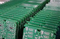
A PCB prototype is a preliminary model of a printed circuit board created during the design and testing phase of electronic product development. It represents the initial attempt to turn a conceptual design into a functional electronic circuit. PCB prototypes are used to validate the design, troubleshoot issues, and refine the layout before scaling up for mass production.

Why are PCB Prototypes Important?
1. Design Validation
Prototypes allow engineers to verify that the design meets functional and performance requirements. This ensures the product behaves as intended.
2. Error Identification
Creating a prototype helps detect and correct design errors or manufacturing issues, saving time and resources in the later stages.
3. Cost and Time Efficiency
Addressing issues during prototyping is far less expensive than fixing them during or after mass production.
4. Iteration and Optimization
Prototyping facilitates multiple iterations, enabling designers to optimize the PCB layout, materials, and components for performance and manufacturability.
Types of PCB Prototypes
1. Proof-of-Concept Prototypes
A Proof-of-Concept prototype is a simplified version of a product created to test and demonstrate its fundamental working principles. Unlike fully functional prototypes, PoC models prioritize concept validation over detailed aesthetics or full feature sets.

2. Functional Prototypes
A Functional Prototype is a near-complete version of a product designed to test its full functionality and performance under real-world conditions. It incorporates all key features, enabling engineers to identify and resolve design issues before production. It Includes all essential components but may not represent the final physical layout.
3. Visual Prototypes
Visual prototypes are early-stage models used to represent and test design ideas. In PCB design, they help validate layouts, component placement, and user interface before production. These prototypes can be 2D sketches, 3D models, or interactive digital models. They aid in stakeholder communication, gather early feedback, and allow for quick iterations without costly physical prototypes. Visual prototypes are essential for ensuring design accuracy and functionality early in the development process.
Visual prototypes can come in various forms, including:
· 2D sketches or drawings: Simple visual representations often used in early concept phases.
· 3D models: Detailed and realistic representations of a product, which can be used to simulate its look and functionality.
· Interactive prototypes: These are digital models that allow for real-time user interaction, commonly used in software or embedded systems development.
4. Pre-Production Prototypes
Pre-production prototypes are working models of a product created before full-scale manufacturing begins. In PCB design, these prototypes serve to test and validate the board's functionality, layout, and performance.
They help identify design flaws, ensure components fit correctly, and test electrical performance. Pre-production prototypes allow engineers to make necessary adjustments before mass production, reducing risks and costs. They are crucial for finalizing designs and ensuring the product meets quality standards and specifications.
Creating a PCB Prototype
1. Design: PCB design software is used to craft the prototype, enabling the creation of precise schematics and detailed layout plans tailored to the project’s requirements.

2. Manufacturing: The prototype is produced through scaled-down manufacturing processes, typically involving a small batch of PCBs made specifically for testing and evaluation purposes.

3. Testing: The prototype is thoroughly tested to verify it meets all required specifications and operates as intended. Testing may include electrical, mechanical, and environmental evaluations.

Key features for designing PCB prototypes:
1. Start with a Clear Design Specification
Before diving into the technical aspects of PCB prototyping, ensure you have a comprehensive design specification.

This document should include:
Functional Requirements: Define the purpose of the PCB and the expected performance parameters.
Mechanical Constraints: Specify size, shape, and enclosure details.
Electrical Requirements: Outline signal integrity, power distribution, and noise control specifications.
Collaborating with stakeholders during this phase reduces the risk of costly redesigns and enhances clarity for manufacturers and assemblers.
2. Choose the Right Materials
Material selection significantly influences a PCB’s performance, durability, and cost. Consider these factors when choosing materials:
Substrate Material: FR4 remains the most popular choice for standard PCBs, but high-frequency designs may require materials like Rogers or polyimide.
Common substrate materials for PCB prototypes include:
1. FR4 (Fiberglass Reinforced Epoxy)
o Features: High durability, good thermal resistance, and cost-effectiveness.
o Applications: Widely used for general-purpose PCBs in consumer electronics.
2. CEM-1 and CEM-3 (Composite Epoxy Materials)
o Features: Similar to FR4 but less expensive; suitable for single-layer or simpler PCBs.
o Applications: Low-cost consumer electronics.
3. Polyimide
o Features: Excellent flexibility, heat resistance, and chemical stability.
o Applications: Flexible and high-temperature PCBs, including aerospace and automotive.
4. Rogers Material
o Features: Superior dielectric properties and low signal loss.
o Applications: High-frequency PCBs like RF and microwave applications.
5. Metal-Core (Aluminum or Copper)
o Features: High thermal conductivity and excellent heat dissipation.
o Applications: LED lighting and power electronics.
6. Ceramic Substrates
o Features: Exceptional thermal conductivity and electrical insulation.
o Applications: High-power and high-frequency circuits.
Copper Thickness: Ensure the copper layer aligns with the board’s current-carrying requirements.
Surface Finish: Opt for finishes like ENIG (Electroless Nickel Immersion Gold) for better solderability and corrosion resistance.
Working closely with your PCB manufacturer ensures that the selected materials meet the functional and budgetary constraints.
3. Design for Manufacturability (DFM)
DFM is critical in ensuring that your PCB design is both functional and easy to produce.

Here are key considerations:
Minimize Complexity: Avoid overly intricate layouts that can lead to manufacturing errors.
Trace Width and Spacing: Adhere to standard design rules to prevent shorts and ensure signal integrity.
Via Selection: Use blind or buried vias only, if necessary, as they add complexity and cost. Via selection in PCB prototyping is critical for ensuring reliable connections between layers.
Various types of vias are used based on design needs:
1. Through-Hole Vias: These extend through all PCB layers, used for general signal routing, power, and ground connections. They are simple and cost-effective but consume space on all layers.
2. Blind Vias: These connect an outer layer to one or more inner layers without passing through the entire board. Ideal for high-density designs where space is limited, they save unused layer space but are more expensive and complex to manufacture.
3. Buried Vias: These connect only internal layers, without reaching the outer layers. They maximize outer-layer space for components but are costly and complex.
4. Micro-vias: These are very small vias connecting adjacent layers, often used in HDI PCBs for high-density interconnects. They enhance routing in tight spaces but require advanced manufacturing processes.
5. Via-in-Pad: These vias are placed directly beneath components like BGAs (Ball Grid Arrays), saving space and improving signal integrity in high-performance applications. However, they are expensive and often need filling and plating.
Selecting the right via type depends on design complexity, cost constraints, and the need for signal integrity. Balancing performance, cost, and manufacturability ensures optimal via selection for PCB prototypes.
Component Placement: Group components logically to simplify routing and reduce assembly errors.

A collaborative review with your PCB manufacturer early in the process can identify potential DFM issues and rectify them before production.
4. Leverage Design for Assembly (DFA)
Designing with assembly in mind can dramatically improve production efficiency. Consider the following:
Component Orientation: Align components consistently to speed up pick-and-place operations.
Clear Labels: Include silkscreen markings for component identification.
Sufficient Clearances: Ensure adequate spacing for automated soldering and testing equipment.
Test Points: Add accessible test points for quality assurance checks.
Involving the PCB assembler during the design phase ensures alignment between design intent and assembly capabilities.
5. Optimize Power and Signal Integrity
As PCBs become more compact and complex, maintaining power and signal integrity is paramount. Consider these best practices:
Ground Planes: Use uninterrupted ground planes to minimize noise and improve signal return paths.
Power Distribution Network (PDN): Optimize the PDN layout to reduce voltage drops and electromagnetic interference (EMI).
Differential Pairs: Route high-speed signals as differential pairs to maintain signal integrity.
Advanced simulation tools can help detect and address issues before prototyping, saving time and resources.
6. Prototype Iteratively
The prototyping process often involves multiple iterations to fine-tune design and functionality. Here’s how to streamline this phase:
Use Rapid Prototyping Services: Partner with manufacturers like PCBGOGO that specialize in quick-turn prototyping.
Test and Validate: Conduct thorough testing after each iteration to identify and resolve issues.
Document Changes: Maintain detailed records of modifications to avoid repeated mistakes and ensure traceability.
Iterative prototyping helps refine the design while keeping costs and timelines under control.
7. Consider Multilayer Designs for Complex Applications
For advanced applications, multilayer PCBs provide the necessary density and functionality.

Key considerations include:
Stack-Up Configuration: Plan the layer stack-up to balance electrical performance and manufacturability.
Impedance Control: Ensure controlled impedance for high-speed signal transmission.
Thermal Management: Use thermal vias and heat sinks to dissipate heat effectively.
Effective thermal management is essential for reliable operation:
· Heat Dissipation: Use thermal vias and heat sinks for components that generate significant heat.
· Copper Planes: Utilize large copper areas to distribute heat across the PCB.
· Material Selection: Choose materials with suitable thermal conductivity.
Collaborating with experienced manufacturers is crucial for achieving the desired performance in multilayer designs.
8. Plan for Scalability
While prototyping focuses on small volumes, keeping scalability in mind ensures a smoother transition to mass production. Key factors include:
Standardized Processes: Use standard design and assembly practices to simplify scaling.
Supplier Collaboration: Establish relationships with reliable component suppliers to avoid shortages.
Cost Optimization: Work with manufacturers to identify cost-saving opportunities without compromising quality.
9. Prioritize Quality Control
Robust quality control processes ensure the reliability of your PCB prototypes. Implement the following measures:
Testing Methods for Ensuring PCB Quality
The final stage of PCB manufacturing involves rigorous testing to ensure the board meets performance and reliability standards. A variety of techniques are employed to identify and address potential defects.
1. Automated Optical Inspection (AOI)
AOI is a crucial step in PCB testing, using high-resolution cameras and image processing algorithms to detect manufacturing defects such as misaligned components, soldering issues, or missing parts. This process is integral during both PCB fabrication and assembly to ensure quality before delivery.

2. Electrical Testing
Electrical tests verify the functionality and integrity of the PCB, focusing on multiple aspects:
· Open and Short Circuit Testing: Ensures there are no unintended disconnections (open circuits) or unintentional connections (short circuits) in the board.
· Capacitance Testing: Measures capacitance values to ensure they align with design specifications.
· Resistance Testing: Evaluates the resistance of components and traces to confirm proper functionality.

· Comparative Testing: Compares the electrical properties of components to reference values, ensuring compliance with design standards.
· Flip Testing: Verifies the correct orientation of components to prevent functionality errors.
· Continuity Testing: Checks for unbroken electrical connections between specific points to confirm proper connectivity.
· Adjacency Testing: Examines the spacing between traces and components to avoid short circuits or interference.
· Impedance Testing: Ensures controlled impedance in high-speed or RF circuits, critical for signal integrity.
· Dielectric Testing: Assesses the insulating properties of the PCB material to prevent electrical breakdown.
3. X-ray Testing
X-ray inspection is employed for complex PCBs, particularly in multilayer designs and assemblies with BGA (Ball Grid Array) components. It detects internal defects such as voids in solder joints, misaligned components, and hidden soldering issues that are not visible with traditional inspection methods.

4. Functional Testing (FCT)
This test simulates real-world operating conditions to verify the PCB’s overall functionality and performance, ensuring it works as intended when integrated into its final application.

5. In-Circuit Testing (ICT): In-Circuit Testing (ICT) is a highly effective method used in PCB manufacturing to verify the integrity and functionality of individual components and circuits on the board. This technique identifies manufacturing defects and ensures the board meets design specifications before deployment.
6. Environmental Testing
Environmental tests, such as thermal cycling, humidity exposure, and vibration testing, simulate the conditions the PCB will face during its lifecycle to assess durability and reliability.
These comprehensive testing methods ensure that every PCB meets stringent quality standards, enhancing reliability and customer satisfaction. Partnering with a quality-focused manufacturer like PCBGOGO enhances the reliability of your prototypes.
10. Iterative Improvement
PCB design is often an iterative process:
· Review: Regularly review the design with the team to identify potential issues.
· Version Control: Track design changes systematically to avoid errors.
· Feedback Integration: Use insights from prototypes and testing to enhance the design.
11. Stay Updated with Industry Trends
The electronics industry evolves rapidly, and staying informed is vital for maintaining a competitive edge. Recent trends include:
Miniaturization:
Embrace smaller components and denser layouts to meet market demands. Miniaturization in PCB design focuses on reducing board size and weight while enhancing functionality, driven by the demand for compact, high-performance devices like smartphones, wearables, and IoT gadgets.

Key Techniques
· HDI Technology: Increases component density using micro-vias and thinner traces.
· Flexible PCBs: Enables compact, foldable designs.
· Multilayer PCBs: Stacks layers for higher functionality in smaller footprints.
· Embedded Components: Integrates components within the PCB substrate to save space.
· Surface-Mount Technology (SMT): Uses smaller, surface-mounted components for denser layouts.
Benefits
· Enables compact, lightweight devices.
· Improves performance with shorter signal paths and reduced EMI.
Challenges
· Thermal management and signal integrity in dense layouts.
· Higher manufacturing complexity and repair difficulty.
Miniaturization drives innovation but requires advanced design and manufacturing techniques to overcome its challenges.
Green Manufacturing:
Adopt eco-friendly materials and processes to align with environmental regulations. Green manufacturing in PCB prototyping focuses on reducing environmental impact by adopting sustainable practices throughout the design and production processes. It emphasizes energy efficiency, waste reduction, and the use of eco-friendly materials.
Key Practices
1. Eco-Friendly Materials: Use lead-free solder, halogen-free laminates, and recyclable substrates like biodegradable polymers or paper-based materials.
2. Energy Efficiency: Optimize manufacturing processes to minimize energy consumption, such as using energy-efficient equipment and renewable energy sources.
3. Waste Reduction: Implement strategies to reduce material waste, including precise cutting techniques, recycling scrap materials, and reusing wastewater.
4. Chemical Management: Adopt safe and eco-friendly chemicals for cleaning and etching processes, ensuring proper disposal of hazardous materials.
5. Process Optimization: Reduce emissions and energy usage through automated and streamlined production methods, such as additive manufacturing.
Benefits
· Decreases carbon footprint and reduces environmental pollution.
· Enhances compliance with global environmental regulations (e.g., RoHS, REACH).
· Improves brand image and attracts eco-conscious customers.
Challenges
· Higher initial costs for eco-friendly materials and equipment.
· Balancing performance and sustainability without compromising quality.
Green manufacturing in PCB prototyping ensures technological innovation aligns with environmental responsibility, paving the way for sustainable electronics production.
Using AI in PCB Prototyping
AI is revolutionizing PCB prototyping by optimizing design, testing, and manufacturing processes, enhancing quality and speeding up production.

Key Applications
1. Design Optimization: AI tools automate design rule checks, optimize component placement, and improve routing for better performance and signal integrity.
2. Predictive Failure Analysis: AI analyzes data to predict potential failures, enabling proactive design adjustments.
3. Generative Design: AI generates efficient PCB layouts based on performance goals and constraints, suggesting optimal component choices.
4. Automated Testing & Inspection: AI-powered AOI and ICT systems detect defects, improving accuracy and reducing human error in inspections. Use AI-powered tools for faster and more accurate defect detection.
5. Thermal & Signal Integrity Simulations: AI simulates and identifies thermal hotspots and signal interference, optimizing PCB designs for stability.
6. Production & Supply Chain Optimization: AI streamlines manufacturing processes, predicts bottlenecks, and optimizes sourcing strategies.
Benefits
· Faster, more efficient design and prototyping processes.
· Higher-quality, defect-free prototypes.
· Reduced costs and time-to-market.
Challenges
· Requires high-quality data for effectiveness.
· Initial setup and training can be expensive and complex.
AI in PCB prototyping improves efficiency, quality, and cost-effectiveness, paving the way for advanced, high-performance PCBs.
Partnering with forward-thinking manufacturers helps you incorporate these innovations into your PCB prototypes.
Why Choose PCBGOGO for Your PCB Prototypes?

PCBGOGO stands out as a trusted partner for PCB prototyping and assembly. With a commitment to quality, speed, and customer satisfaction, PCBGOGO offers:
Quick-Turn Prototyping: Rapid delivery without compromising on quality.
Comprehensive Services: From design reviews to final assembly, PCBGOGO supports you every step of the way.
Cutting-Edge Technology: State-of-the-art facilities ensure precise and reliable manufacturing.
Global Reach: Serving clients across diverse industries worldwide.
Partner with PCBGOGO to streamline your prototyping journey and bring your ideas to life.
Conclusion
Designing PCB prototypes requires a strategic approach that balances innovation, practicality, and cost-effectiveness. By focusing on clear specifications, robust design principles, and collaborative partnerships, manufacturers and assemblers can create high-quality prototypes that pave the way for successful products. With expert support from a trusted partner like PCBGOGO, you can navigate the complexities of PCB prototyping with confidence and precision.


