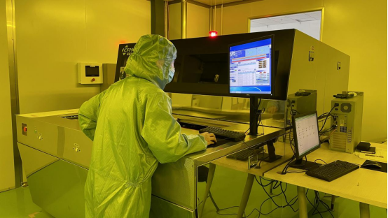
Instrumentation PCB Low Temperature Drift Challenge: Material and Process Optimization and Stable Solutions
Instrumentation PCBs are widely used in industrial control, outdoor monitoring, and medical equipment, where reliable operation across a wide temperature range of -40°C to 85°C is required. In such environments, low-temperature drift directly affects measurement accuracy and long-term system reliability.
Industry data shows that PCBs without low-temperature drift optimization can experience:
2%–5% resistance variation with a 10°C temperature change
Capacitance deviation exceeding 10%, leading to doubled measurement errors
With nearly 10 years of experience in the electronics manufacturing industry, PCBGOGO leverages four self-owned production bases, advanced environmental testing equipment, and material R&D capabilities to deliver low-temperature drift optimized PCB solutions for instrumentation customers, including Haier, Joyoung, and Yuwell.
This article analyzes the key factors influencing low-temperature drift and presents practical, full-process optimization strategies covering material selection, manufacturing processes, and design improvements.

Low Temperature Drift Influencing Factors and Industry Standards
Core Evaluation Metrics for Low Temperature Drift
Low-temperature drift performance in instrumentation PCBs is typically evaluated using three critical indicators:
Temperature Coefficient of Resistance (TCR)
Copper foil TCR ≤ 1.5 × 10?? /°C (IPC-4562)Dielectric Constant Stability
Dielectric constant fluctuation ≤ ±0.05 for a 10°C temperature changeDimensional Stability
Board thickness change rate ≤ ±0.5% after temperature cycling
(GB/T 4677-2017, Clause 5.8)
Key Factors Affecting Low Temperature Drift
Substrate Material
Standard FR-4 exhibits higher dielectric constant variation and TCR, making it a major contributor to low-temperature drift. High-TG, low-loss substrates such as Shengyi S1130 and Rogers RO4350B offer significantly improved stability.
Copper Foil Characteristics
Electrolytic copper foil has a higher TCR than rolled copper foil. Inconsistent copper thickness can cause uneven thermal distribution and accelerate resistance drift.
Process Control
Non-uniform lamination temperature and incomplete resin curing introduce residual stress. During temperature changes, stress release leads to deformation and electrical instability.
Surface Treatment
Traditional tin plating is prone to embrittlement at low temperatures, increasing contact resistance. Immersion gold and immersion silver provide better low-temperature stability.
Common Industry Misconceptions
Focusing solely on substrate selection while ignoring copper foil and process control
Relying only on room-temperature test results without environmental aging tests
Overlooking temperature compensation circuits in design and depending entirely on PCB material performance
Full-Process Optimization Strategy for Low-Temperature Drift PCBs
Material Selection: Controlling Temperature Sensitivity at the Source
Substrate Recommendations
Industrial instrumentation: Shengyi S1130 (TG 170°C, TCR 1.2 × 10?? /°C), dielectric fluctuation ≤ ±0.04 from -40°C to 85°C
Medical-grade instrumentation: Rogers RO4350B (TG 280°C, TCR 8 × 10?? /°C), industry-leading dielectric stability
All PCBGOGO substrates comply with ROHS and REACH, with free material samples available for validation.
Copper Foil Selection
Rolled copper foil (Ra ≤ 0.2 μm)
Inner layers: 2 oz (70 μm)
Outer layers: 1 oz (35 μm)
Copper thickness uniformity deviation is controlled within ±5% using precision measurement tools.
Surface Treatment
Medical instruments: Immersion gold, gold thickness ≥ 1 μm
Industrial instruments: Immersion silver to avoid low-temperature tin embrittlement
Surface treatment thickness deviation is controlled within ±0.1 μm via fully automated plating systems.
Process Optimization: Reducing Residual Stress Through Intelligent Manufacturing
Lamination Process
Heating gradient: 5°C/min
Curing temperature: 180°C
Holding time: 120 minutes
Cooling: Natural cooling, ≤ 3°C/min
This ensures full resin curing and minimizes internal stress.
Etching Process
Spray etching at 45 ± 2°C
Etching rate: 2 μm/min
AOI online inspection ensures uniform line width and etching accuracy.
Molding Process
CNC molding with cutting speed 50 mm/s
Post-molding deburring to reduce edge stress concentration.
Design Optimization: Temperature Compensation and Structural Stability
Circuit Design
Incorporation of temperature compensation resistors (e.g., PT1000) in precision sampling circuits
PCBGOGO engineers provide joint PCB and circuit optimization support.
Structural Design
Thermal expansion compensation gap ≥ 0.5 mm at PCB edges
Critical components (oscillators, sensors) placed near the PCB center to reduce edge temperature effects.
Routing Design
Power traces ≥ 1 mm to reduce Joule heating
Continuous ground copper pours to stabilize ground potential during temperature changes.
Testing and Verification: Simulating Real Operating Environments
Environmental Testing
Temperature cycling from -40°C to 85°C
100 cycles, 2 hours per cycle
Post-test impedance and insulation resistance fluctuation ≤ ±3%
Mechanical Stress Testing
Copper peel strength ≥ 1.5 N/mm (IPC-6012)
Dimensional Stability Testing
Board thickness and line width change rate ≤ ±0.3%, verified using high-precision 2D measurement systems.
Conclusion: A Systematic Approach to Low-Temperature Drift Control
Effective low-temperature drift control for instrumentation PCBs requires an integrated strategy covering materials, manufacturing processes, design optimization, and environmental testing.
By selecting temperature-stable materials, minimizing residual stress through precise process control, and enhancing performance with design-level compensation, manufacturers can achieve stable, repeatable performance across extreme temperature ranges.
As a leading PCB and PCBA manufacturer, PCBGOGO combines advanced materials, intelligent production systems, and comprehensive testing capabilities across its four production bases to deliver one-stop low-temperature drift solutions—from customized material selection to precision manufacturing and environmental verification.

