How to control the quality of PCB gold finger plating?
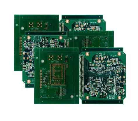
In the high-stakes world of electronic manufacturing, the interface between a PCB and its system connector is a frequent point of failure. PCB gold finger plating serves as the critical bridge in this equation, providing the wear resistance and conductivity required for high-performance edge connectors. Because these components are subject to repeated insertion and removal, the quality of the plating process is paramount to the longevity of the device.
To ensure your boards meet international standards like IPC-4522, manufacturers must implement a multi-layered approach to quality control.

Chemical Composition and Solution Purity
The "heart" of the plating process is the electrolytic bath. Maintaining PCB gold finger plating quality starts with the chemical equilibrium of the gold and nickel tanks.
Contamination Control: Metallic impurities (such as copper or iron) in the gold bath can lead to discoloration and increased contact resistance. Constant carbon filtration and periodic lab analysis are mandatory.
Hardness Additives: Unlike immersion gold (ENIG), gold fingers require "Hard Gold." This involves adding small amounts of cobalt or nickel to the gold deposit to increase its Vickers hardness, ensuring the fingers don't wear down after hundreds of mating cycles.
The Science of Process Parameters
Precision is what separates a reliable board from a defective one. Controlling the physics of the plating tank is just as important as the chemistry.
Current Density Distribution: Uneven current distribution can cause "dog-boning" effects, where the gold is thicker at the edges and thinner in the middle. Advanced racking systems and "thieving" traces are used to balance the electrical load.
Thermal Stability: The chemical reaction rates are highly sensitive to temperature. Automated thermal controllers keep the bath within a narrow window (typically ±2℃) to ensure a consistent grain structure.
Surface Preparation and Adhesion
A gold layer is only as strong as its bond to the substrate. Before the gold is applied, a critical nickel underplating must be executed.
Barrier Layer: The nickel layer (usually 100-200 micro-inches thick) acts as a diffusion barrier, preventing copper from migrating into the gold and oxidizing.
Pre-Cleaning: Any residual oils, fingerprints, or oxides on the copper surface will lead to delamination. A rigorous series of micro-etching and acid washes ensures the surface is chemically active and ready for bonding.
Advanced Inspection and Verification
To guarantee that the PCB gold finger plating meets design specifications, a robust post-production testing protocol is implemented:
XRF Testing: X-ray Fluorescence is used to non-destructively measure the thickness of both the nickel and gold layers at multiple points along the connector.
Tape Testing: A standardized adhesion test ensures the gold does not flake under mechanical stress.
Porosity Testing: Especially in harsh environments, checking for pores in the gold layer is vital to prevent underlying nickel corrosion.
Conclusion: Why Quality Control is Non-Negotiable
For engineers designing for 5G, aerospace, or automotive applications, the margin for error is zero. Poorly executed plating leads to intermittent signals, data loss, and eventual system failure. By focusing on bath purity, strict parameter control, and meticulous surface preparation, manufacturers can deliver a product that exceeds expectations.
The mastery of PCB gold finger plating is a hallmark of a high-quality fabricator. As devices become faster and more compact, the reliability of these golden connections remains the foundation of modern electronic architecture. For those seeking industry-leading precision and reliability in their high-frequency or high-speed designs, PCBGOGO provides professional-grade gold finger solutions that meet the most demanding technical specifications.

