How to Manufacture Dual-Section Gold Fingers on a PCB?
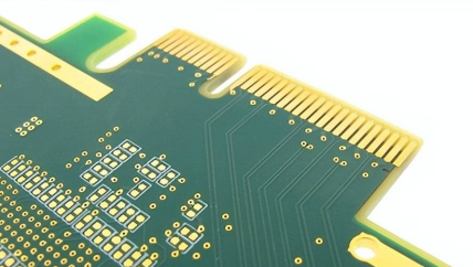
In high-frequency, data-sensitive electronic equipment, the stability of connection terminals determines the reliability of the entire system. Compared to standard single-layer structures, the dual-section gold fingers (also known as split gold fingers) utilize front and back segmented plating and geometric differences. This design ensures a "ground/power first, data signal second" contact sequence, which significantly reduces interference during hot-plugging and enhances long-term wear resistance.

1. Structure and Mechanism of Dual-Section Gold Fingers
The core of dual-section gold fingers lies in regional partitioning and segmented plating:
Front Section (Contact Zone): Makes contact first. It usually handles ground or power references and requires high wear resistance.
Rear Section (Signal/Soldering Zone): Makes contact later. It transmits control signals, data, or functional pins.
This stepped structure is widely used in PCIe cards, DDR modules, M.2 expansion boards, and industrial control backplanes.
2. Design Specifications and Parameters
To avoid manufacturing errors, it is recommended to include these parameters in your FAB notes or Gerber files.
Segmented Design and Plating Structure
Geometry and Beveling
Front Bevel: Typically 30° or 45° (±1°).
Rear Form: Right angle or micro-bevel (≤0.1mm).
Length Difference: A gap of 0.3~0.6mm (0.5mm is recommended for standard connectors).
3. The Manufacturing Process
The key to producing dual-section gold fingers is the use of dual-plating and precise masking control.
Preparation: Material cutting and multilayer lamination.
Window Opening: Solder mask removal and cleaning.
Base Prep: Micro-etching and copper coarsening.
First Plating: Nickel and Hard Gold plating for the front section.
Masking: Applying protective film or exposure-based protection.
Second Plating: Plating the rear section with the required finish.
Final Protection: Film removal and OSP (Organic Solderability Preservative) application.
Mechanical Finishing: CNC beveling, deburring, and edge smoothing.
Quality Control: XRF gold thickness testing and visual inspection.
4. Common Risks and Prevention
5. Application Scenarios
The dual-section gold fingers structure is the preferred choice for:
AI acceleration cards and server motherboards.
Industrial modules and high-speed network switches.
Gaming console interfaces.
Any interface sensitive to signal jitter or requiring hot-plugging capabilities.
Conclusion
Creating dual-section gold fingers is more than just applying two types of metal; it is a systematic approach to contact sequencing, plating precision, and structural geometry. Aligning your design specifications with your PCB manufacturer's capabilities is the most critical step to avoiding rework.
For your next high-reliability project, ensure all critical values are embedded in your Gerber files to minimize deviation. At PCBGOGO, we specialize in advanced edge connector solutions, ensuring your high-speed designs meet the toughest durability standards.

