
How to Laser Cut Stencils for High-Precision PCB Assembly?
In modern SMT assembly, laser-cut stencils are essential for achieving accurate solder paste deposition and ensuring stable production yields. Whether you're a hardware engineer, PCB designer, or electronics manufacturer, understanding how to laser cut stencils and what to consider during the process can significantly improve the quality of your assembly results.
This guide explains what a laser-cut stencil is, how the cutting process works, and the key points you must pay attention to—plus why many professionals choose PCBGOGO for high-precision laser stencils.
1. What Is a Laser-Cut Stencil and Why Use It?
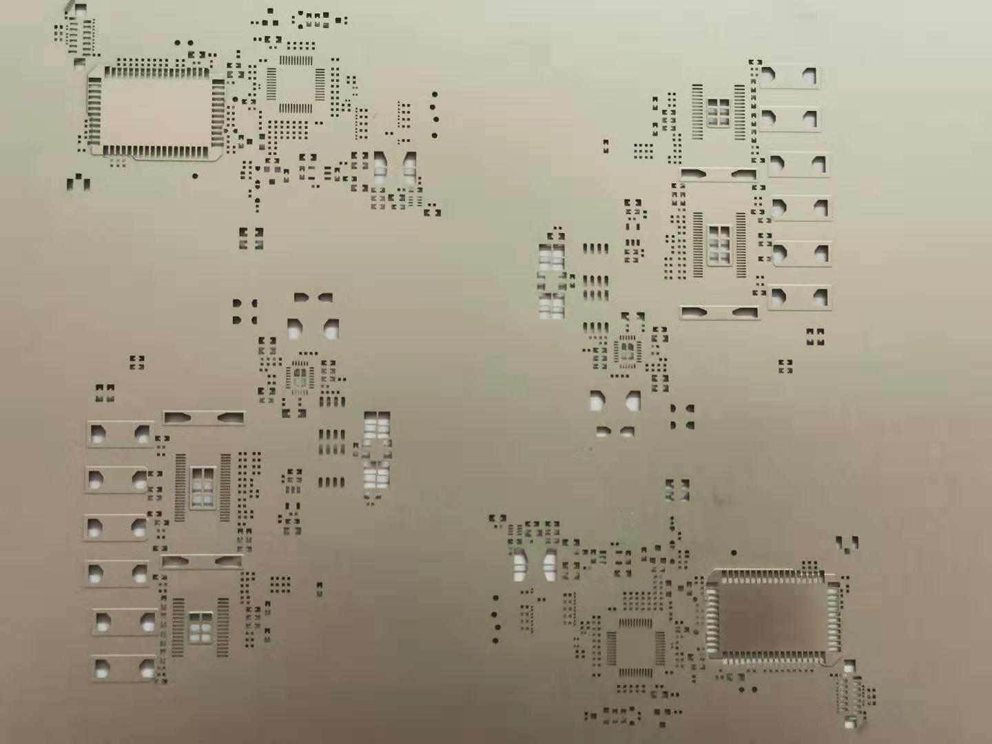
A laser-cut stencil is a stainless-steel sheet with precisely cut apertures used to transfer solder paste onto PCB pads during SMT assembly. The apertures dictate how much solder paste is deposited, making stencil accuracy critical for preventing defects like bridging, insufficient solder, or tombstoning.
Why Use Laser-Cut Stencils?
Ultra-High Precision
Laser cutting allows aperture accuracy of ±3–5 μm, making it ideal for fine-pitch components, BGAs, QFNs, and 01005/0201 packages.
Clean, Smooth Aperture Walls
The laser beam melts the edges of the metal, forming smooth internal walls that improve solder paste release.
Flexibility in Aperture Shapes
Laser-cutting supports optimized shapes such as:
Home-plate apertures
Windowpane patterns
Rounded corners
Modified apertures for thermal pads
Stable and Repeatable Quality
Because apertures are digitally programmed, laser stencils offer excellent consistency, especially for high-density PCB designs.
2. How to Laser Cut Stencils (Step-by-Step Process)
Understanding how to laser cut stencils helps ensure better design decisions and higher-quality PCB assembly. Below is the typical workflow used by professional stencil manufacturers.
Step 1 — Import and Prepare the Gerber Files
Stencil engineers begin by reviewing the PCB’s Gerber data. They adjust aperture dimensions according to:
Component type (BGA/IC/QFN)
Pad geometry
Recommended solder paste release
Stencil thickness
Any required aperture reduction or enlargement
This ensures the stencil matches the PCB printing requirements.
Step 2 — Select the Stainless-Steel Material
High-quality 304 or 316 stainless steel is used because of its durability, flatness, and excellent paste release performance.
Common thicknesses:
0.10 mm – 0.15 mm for general SMT
0.08 mm for ultra-fine-pitch components
0.18–0.20 mm for large pads or power devices
Step 3 — Laser Cutting the Apertures
A precision fiber laser cuts each aperture according to the digital design.
Key characteristics of laser cutting:
Accuracy: ±3–5 μm
Minimal heat distortion
Consistent aperture size and shape
Supports complex and non-standard patterns
The laser essentially vaporizes the metal, forming clean, sharp openings.
Step 4 — Post-Treatment (Optional but Recommended)
After cutting, stencils may undergo:
Electro-polishing
Smooths micro-burrs and improves solder paste release.
Nano-coating
Applies a surface coating that prevents clogging and enhances printing consistency—especially useful for fine-pitch designs.
Step 5 — Final Inspection and Quality Control
Before shipping, professional manufacturers inspect:
Aperture dimensions
Wall consistency
Stencil tension and flatness
Frame alignment accuracy
Surface finish
This ensures the stencil meets IPC-7525 standards and performs reliably in production.
3. What to Pay Attention to When Laser Cutting Stencils
To produce a high-performance SMT stencil, consider the following critical points:
Aperture Size Adjustment
Improper aperture size may cause:
Solder bridging (too large)
Insufficient solder (too small)
Each pad type may require a reduction or enlargement percentage.
Stencil Thickness Selection
Thickness directly influences solder volume.
General rules:
Thin stencil = better for fine-pitch
Thick stencil = better for large components
Material Quality and Flatness
Low-grade steel or warping causes uneven paste transfer, leading to print defects.
PCB Pad Design Accuracy
If the PCB footprint is inaccurate, even the best stencil will not produce correct solder deposit results.
For High-Density PCBs, Consider Nano-Coating
This significantly reduces clogging and ensures consistent printing for tiny apertures.
Frame Type
Choose between:
Framed stencils (for large-scale production)
Frameless stencils (for prototypes or manual printing)
Conclusion: Why Choose PCBGOGO for Laser-Cut Stencils?
A high-quality stencil is essential for clean, precise solder paste printing, especially as components continue to shrink and PCB designs become more complex. Understanding how to laser cut stencils helps you make smarter decisions in PCB manufacturing and assembly.
PCBGOGO provides:
±5 μm precision laser cutting
Professional aperture optimization
Electro-polishing & nano-coating options
Fast global delivery
Affordable pricing for prototypes & production runs
Whether you need a rapid prototype or full-scale SMT production, PCBGOGO offers reliable, high-precision laser stencils to ensure your assembly achieves the highest quality.

