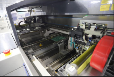
How to Identify and Prevent Solder Joint Cracks in SMT Assembly?
SMT (Surface Mount Technology) is the cornerstone of modern electronics manufacturing, widely utilized in consumer electronics, automotive systems, and telecommunications. However, the integrity of a board is only as strong as its connections. A persistent issue in the industry is the solder joint cracks, defects that severely compromise the quality and long-term reliability of PCBA (Printed Circuit Board Assembly) products. Understanding why these cracks occur and how to prevent them is essential for any high-reliability project.

1. Analysis of Primary Causes for Solder Joint Cracks
A solder joint crack rarely stems from a single source; it is usually the result of a combination of material, process, and equipment failures.
Material Issues
Solder Paste Quality: The composition of the paste directly dictates the bond's strength. Low-quality or expired solder paste often suffers from poor fluidity, leading to brittle joints. Furthermore, insufficient flux activity prevents the solder from properly bonding with component leads.
PCB Substrate Materials: The base material and surface finish (such as OSP, ENIG, or HASL) play a vital role. If a substrate has poor heat resistance or an incompatible Coefficient of Thermal Expansion (CTE), internal stresses will build up during the heating cycle, triggering fractures.
Component Reliability: Substandard components with poor lead plating or improper thermal expansion properties can expand or contract unevenly during high-temperature soldering, resulting in a visible or microscopic solder joint crack.
Process & Thermal Issues
Improper Reflow Temperature Profile: Temperature control is the heart of reflow soldering. If the peak temperature is too low, the solder fails to melt completely (cold soldering); if it is too high, it creates excessive intermetallic compound (IMC) growth, making the joint brittle.
Soldering Stress: During the cooling phase, materials with different thermal expansion rates contract at different speeds. In large-scale or thick PCBs, this thermal stress is a leading cause of joint failure.
Poor Process Control: Errors in solder paste printing (uneven thickness) or component placement (offset) lead to uneven force distribution across the joint, eventually causing it to snap under pressure.
Equipment Factors
Aging Reflow Equipment: If a reflow oven lacks temperature uniformity or has failing heating elements, the board will experience "hot spots" or "cold spots," leading to inconsistent solder quality.
Printer Inaccuracy: If the stencil printer lacks precision, the volume of solder paste will vary across the board, leaving some joints too thin to support the mechanical load.
2. Strategic Solutions and Prevention
To eliminate the risk of a solder joint crack, manufacturers must adopt a multi-layered defense strategy.
Material Improvement Strategies
High-Quality Solder Paste: Only use high-grade pastes with excellent wetting properties. Strictly monitor expiration dates and storage temperatures to ensure the flux remains active.
Substrate Optimization: Select PCB base materials with low CTE and high heat resistance based on the product's end-use environment. Improving surface finishes (like using gold or silver plating with anti-oxidation properties) can also enhance bond reliability.
Strict Component Sourcing: Manage your supply chain rigorously. Choose components with proven solderability and thermal properties that match your specific solder alloy.
Process Optimization
Reflow Curve Calibration: Tailor the reflow profile to the specific board density. Ensure the preheat, soak, and reflow zones allow for complete melting while the cooling zone provides a smooth transition to avoid "thermal shock."
Stress Management: Implement "step-heating" or controlled cooling rates to alleviate the stress caused by inconsistent thermal expansion.
Real-time Monitoring: Use AOI (Automated Optical Inspection) and X-ray inspection to detect placement offsets or internal joint voids early in the production line.
Maintenance and Training
Regular Equipment Maintenance: Calibrate reflow ovens and stencil printers monthly to ensure temperature stability and printing precision.
Technical Training: Ensure operators are well-versed in the nuances of solder paste behavior and equipment parameters. Human error is often the "silent" contributor to soldering defects.
Summary
In the complex environment of electronics manufacturing, a solder joint crack is the cumulative result of material, process, and equipment variables. By selecting high-quality materials, fine-tuning the reflow temperature profile, and maintaining strict process discipline, you can significantly enhance the durability of your PCBA.
PCBGOGO provides industry-leading SMT assembly services, specifically engineered to prevent solder joint cracks. Our state-of-the-art equipment and rigorous quality control protocols ensure that every joint is robust, reliable, and built to last. Place a quote now!

