
How PCB Vias Connect Different Layers
Ever wondered how the lines on a complex motherboard connect between different layers? The secret lies in vias. Think of them as the "elevators" or "stairs" that allow signals to travel between a circuit board's layers.
What Is a PCB Via?
A via is a small, plated hole that connects copper traces on different layers of a multi-layer PCB. They are crucial for:
Making Connections: Creating electrical links between layers.
Enabling High-Density Design: Allowing signals to change layers, which saves surface space and enables more compact designs.
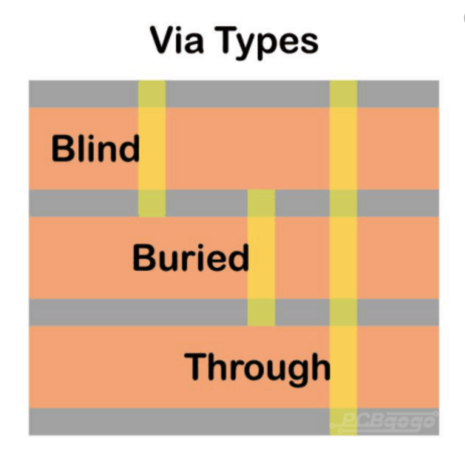
Three Main Types of Vias
There are different types of vias for different design needs:
Through-Hole Vias: The most common type. They go all the way through the board, connecting all layers.
Blind Vias: These only connect an outer layer to one or more inner layers, but don't go through the entire board.
Buried Vias: These connect two or more inner layers and are not visible from the outside. They are used for the highest-density routing.
At PCBgogo, we know that vias are the lifeblood of a circuit. Our professional manufacturing process ensures precise production of all via types, guaranteeing a stable and reliable design for your product.

