
How Can Manufacturers Optimize Solder Void Reliability in SMT Assembly?
In the pursuit of high-quality electronics, the integrity of every solder joint is paramount. One of the most critical and challenging defects to manage in Surface Mount Technology (SMT) is the formation of solder voids—small, gas-filled cavities trapped within the solder joint after reflow. While completely eliminating voids is often impractical, controlling their size and distribution is vital. Research into Solder Void Reliability is crucial because these discontinuities significantly compromise the mechanical strength, thermal dissipation, and long-term stability of the PCBA, posing a major risk, particularly in high-reliability applications like automotive and aerospace electronics.
Defining and Identifying Solder Voids
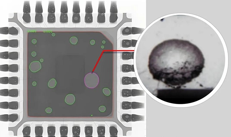
A solder void is a visible gap or pore within the finished solder fillet, formed by trapped gases. The presence of voids is measured by Void Rate, which is the total void area expressed as a percentage of the entire solder joint area.
Why Voids Threaten Reliability:
Reduced Thermal Conductivity: Voids act as thermal insulators. In power components (e.g., QFNs, BGAs with thermal pads), voids obstruct the primary heat path from the component to the PCB, leading to localized overheating and premature failure.
Compromised Mechanical Strength: Voids reduce the effective cross-sectional area of the solder joint, making it susceptible to cracking under thermal cycling stress (expansion and contraction).
Electrical Failure: While less common, very large voids or void clusters can disrupt the electrical path, leading to intermittent or complete circuit failure over time.
Root Causes of Void Formation
Controlling Solder Void Reliability requires a multi-pronged approach that addresses the primary sources of gas entrapment:
Solder Paste Formulation Issues:
Flux Volatilization: The flux in the solder paste is designed to clean surfaces and then escape during reflow. If the paste's rheology (viscosity and flow properties) or the flux activity is incorrect, gases can become trapped.
Improper Handling: Suboptimal storage, temperature cycling, or insufficient stirring can lead to uneven mixing of the solder powder and flux, causing localized gassing during the reflow process.
PCB Surface and Pad Contamination:
Oxidation and Moisture: Oxidized copper pads or excessive moisture trapped within the PCB material can react with the molten solder, generating gas bubbles. Even microscopic contamination can destabilize the interface.
Surface Finish: The type and quality of the PCB pad finish (e.g., HASL, ENIG, OSP) affect the wettability of the solder, influencing how easily trapped gas bubbles can escape.
Reflow Profile Optimization:
Preheat Stage: The preheat zone of the reflow oven is crucial. If the temperature ramp rate is too fast, the flux can rapidly volatilize and trap gases before they can vent. Proper reflow curve profiling allows sufficient time for flux activation and gas escape before the solder melts (reaches liquidus).
Industry Standards for Void Acceptance
Acceptable void rates are dictated by industry standards (like IPC-A-610) and the product's classification, reflecting the required Solder Void Reliability:
Manufacturers must use X-ray inspection (2D or 3D CT) to accurately quantify the void percentage in critical solder joints, such as those under Ball Grid Arrays (BGAs) and thermal pads of components like QFNs and LGAs.
Mitigation Strategies
To enhance Solder Void Reliability, manufacturers must implement advanced control techniques:
Vacuum Reflow Soldering: Utilizing a vacuum during the liquid phase of the reflow profile is the most effective method, as the reduced atmospheric pressure mechanically forces trapped gas bubbles out of the molten solder.
Nitrogen Atmosphere: Using a nitrogen-filled reflow oven inhibits oxidation, improving solder wettability and allowing gases to escape more freely.
Stencil Design Optimization: Modifying the stencil aperture design for thermal pads, often using a "window pane" pattern, provides dedicated escape routes for volatile flux components.
Conclusion
Maintaining high Solder Void Reliability is a sophisticated challenge in modern SMT assembly that requires precise process control, material quality management, and advanced inspection technology. By rigorously addressing the causes related to solder paste handling, PCB surface quality, and reflow profile integrity, manufacturers can ensure the longevity and performance of their electronic devices. For those seeking partners with expertise in achieving the lowest possible void rates for complex, high-reliability PCBAs, PCBGOGO is your ideal choice. We specialize in precise SMT assembly manufacturing, employing optimized reflow processes and utilizing X-ray inspection to guarantee the Solder Void Reliability and structural integrity required for even Class 3 products. Contact us now at service@pcbgogo.com.

