
 日本語
日本語

High-Speed PCB Reliability in Extreme Environments: A Practical Engineer’s Guide to Anti-Aging and Stability Optimization
Introduction
Outdoor consumer electronics—such as surveillance cameras, portable 5G routers, and in-vehicle smart terminals—demand high-speed PCBs that can withstand harsh environmental conditions. These include -40°C to 85°C temperature ranges, 95% RH humidity, and 10g vibration shocks. Reliability requirements are significantly higher than those for indoor devices.
Industry data shows that high-speed PCBs without environmental hardening often fail within 6–12 months, with field failure rates reaching 25%. One outdoor camera manufacturer even reported an 18% repair rate due to corrosion-induced PCB failures in high-temperature and high-humidity conditions.
PCBGOGO has specialized in extreme-environment PCB manufacturing, providing comprehensive solutions integrating weather-resistant materials, anti-aging processes, and structural reinforcement. Its automotive and industrial PCBs have passed -40°C to 85°C and 1000-hour temperature/humidity cycle tests, achieving outdoor lifespans of 5+ years.
This guide—based on IPC-9701 and GB/T 2423 standards—breaks down the exact steps engineers should take to improve high-speed PCB reliability in extreme environmental conditions.
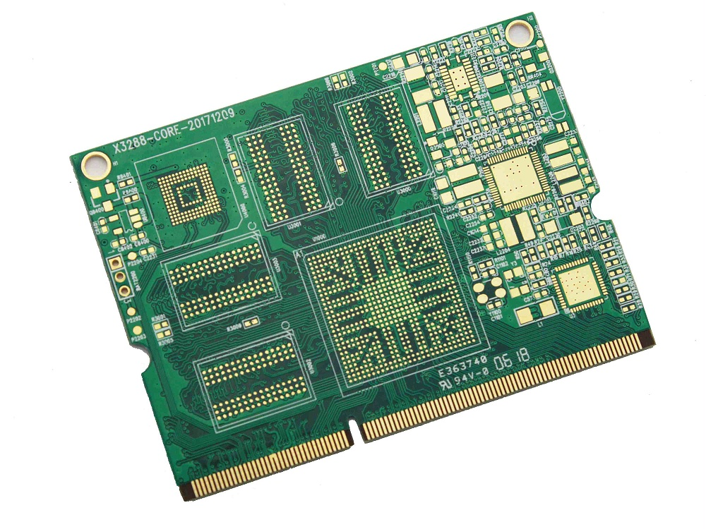
2. Technical Overview: How Extreme Environments Impact High-Speed PCB Reliability
2.1 Types of Extreme Environments and Their Effects
Extreme operating conditions fall into three main categories:
1. Temperature & Humidity
Wide temperature cycles cause expansion/contraction stress.
High humidity leads to PCB moisture absorption and metal corrosion.
According to GB/T 2423.4, outdoor devices must survive 40°C, 95% RH for 1000 hours without corrosion or performance loss.
2. Vibration & Mechanical Shock
Transport and operation vibrations can lead to:
Solder joint cracking
Via barrel fractures
Component/connector loosening
3. Chemical & Salt Corrosion
Outdoor salt spray and industrial dust cause:
Oxidation
Surface finish degradation
Increased contact resistance
2.2 Failure Mechanisms in Extreme Environments
Temperature & Humidity Failures
Dielectric constant drift due to moisture absorption (≥10%) → impedance mismatch
Pad oxidation (CuO ≥ 0.5 μm) → weak solder joints
PCB warpage (≥0.3 mm) or delamination from thermal stress
Vibration Failures
Fatigue cracks in solder joints (≥0.1 mm)
Via copper fractures → intermittent or permanent open circuits
Corrosion Failures
Salt spray corrosion area ≥5%
Gold layer thinning (≤0.5 μm)
Contact resistance rising significantly
2.3 How PCBGOGO Ensures Extreme-Environment Reliability
PCBGOGO applies three layers of protection:
Material Durability
Shengyi S1130 FR4 (≤0.2% moisture absorption)
Rogers RO4350B (?55°C to 150°C)
Process Reinforcement
ENIG or immersion gold
Conformal coating application
Salt-spray test pass rate: 100%
Structural Optimization
Reinforced vias
Stiffeners
Verified using 10g/11ms half-sine vibration tests
3. Practical Solutions: Step-by-Step Guide to Extreme-Environment PCB Reliability Optimization
3.1 Material Selection: Weather Resistance & Anti-Aging
Key requirements
Choose PCB materials based on environmental type (temperature, humidity, vibration, corrosion).
Avoid “one-material-fits-all” design mistakes.
Recommended specifications
Temperature/Humidity: Shengyi S1130 FR4 (?40°C to 125°C, ≤0.2% moisture absorption)
Salt/Fog environment: Rogers RO4350B + ENIG (≥1.5 μm gold thickness)
High vibration: High Tg materials (Tg ≥ 170°C)
Compliances: IPC-4101, GB/T 4677
3.2 Process Optimization: Anti-Corrosion & Anti-Vibration Enhancement
Anti-corrosion protection
Apply conformal coating (e.g., Dow Corning DC1-2577)
Coating thickness: ≥50 μm
Salt-spray test 48h per GB/T 2423.17 — no corrosion allowed
Anti-vibration hardening
Reinforced vias (0.4 mm diameter, 5 mm spacing)
FR4 stiffeners (1.0 mm thickness)
Rounded solder joints to reduce fatigue
IPC-610G Class 3 manufacturing criteria
3.3 PCB Design Optimization: Reducing Environmental Stress
Thermal & mechanical structural design
Distribute high-power components to avoid hot zones
PCB corners: rounded (radius ≥2 mm)
Add drainage holes (1 mm) to prevent water accumulation
Increase copper pour area to ≥30% of PCB
Use ≥2 oz copper for stable thermal cycling
Tools: PADS, ANSYS Mechanical stress simulation
3.4 Verification: Complete Environmental Reliability Testing
Test Conditions
Temperature/Humidity Cycling (GB/T 2423.22):
-40°C to 85°C, 1000 cycles, warpage ≤0.1 mmVibration Test (GB/T 2423.10):
10g, 11 ms half-sine — no solder or via cracksSalt Spray (GB/T 2423.17):
5% NaCl, 48 hours — no visible corrosion
4. Case Study: Outdoor 5G Router PCB Reliability Improvement
4.1 Initial Problems
A consumer electronics brand used an 8-layer 10Gbps PCB. Testing revealed:
Warpage 0.4 mm after 500 cycles
30% solder joint cracking & 12% via failure
Salt-spray corrosion area 8%; contact resistance 0.1 Ω
4.2 PCBGOGO Optimization Actions
Material
Upgraded to Shengyi S1130 FR4 (Tg 170°C, 0.15% moisture absorption)
ENIG with 1.8 μm gold layer
Industrial-grade components (?40°C to 85°C)
Process
60 μm Dow Corning DC1-2577 conformal coating
1.0 mm FR4 stiffeners
Reinforced vias; via copper thickness 30 μm
Design
Re-distributed hot components
2 mm rounded edges
4 drainage holes
40% copper area, 2 oz copper
Testing
All tests passed at PCBGOGO’s reliability lab:
1000 temperature/humidity cycles
10g vibration
48h salt fog
4.3 Results
Warpage reduced to 0.08 mm
Dielectric drift only 3%
Solder cracking rate dropped to 0.2%
Field failure rate reduced from 25% → 2.5%
Outdoor lifespan extended to 5+ years
Monthly sales exceeded 30,000 units
Conclusion
Ensuring high-speed PCB reliability in extreme environments requires a systematic approach integrating:
Weather-resistant and environment-matched materials
Anti-aging manufacturing processes (coatings, surface treatments, reinforced vias)
Structural and layout design to reduce environmental stress
Full-spectrum testing to validate reliability
PCBGOGO’s advanced materials, precision manufacturing, and reliability testing capabilities help engineers build high-speed PCBs that survive harsh environments and achieve long operational lifespans.




