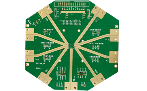
High-Frequency PCB Stack-Up Design: Material Selection and Impedance Control
In high-frequency electronics, such as 5G communications, RFID, and satellite navigation, the main challenge of high-frequency PCB stack-up design is minimizing signal loss and achieving precise impedance control. Both objectives rely heavily on proper material selection and scientific impedance management strategies. PCBGOGO, as a professional high-frequency PCB manufacturer, leverages deep understanding of material properties and design processes to deliver stack-up solutions optimized for high-frequency applications.

1. Material Selection for High-Frequency PCBs
Material choice is the first critical step in high-frequency PCB stack-up design. The focus is on three key parameters: dielectric constant (Dk), dissipation factor (Df), and coefficient of thermal expansion (CTE).
Dielectric constant (Dk) directly affects signal propagation speed; lower Dk values allow faster transmission.
Dissipation factor (Df) determines signal energy loss; lower Df reduces high-frequency attenuation.
Thermal expansion (CTE) influences reliability during thermal cycles.
For 5G millimeter-wave PCBs, PCBGOGO typically selects PTFE-based materials, with Dk around 2.1 and Df as low as 0.0009, significantly reducing signal attenuation. For cost-sensitive applications, modified high-TG FR-4 materials (Dk ≈ 3.8, Df ≈ 0.018) provide a balanced trade-off between performance and cost.
2. Copper Foil Considerations for High-Frequency Signals
Copper foil selection is equally critical in high-frequency PCB stack-up design. Due to the “skin effect,” high-frequency signals primarily travel along the conductor surface. Therefore, copper foil with low surface roughness, such as very-low-profile (VLP) copper, is preferred.
PCBGOGO uses VLP copper with roughness Ra ≤ 1.0 μm, compared to standard copper Ra ≥ 3.0 μm. This reduces skin-effect losses and improves high-frequency signal transmission efficiency.
3. Impedance Control Strategies
Impedance control is central to high-frequency PCB stack-up design. High-frequency signals are highly sensitive to impedance variations. Mismatched impedance can cause signal reflection, crosstalk, and system failures.
Microstrip Lines (signal on PCB surface with a ground reference plane) impedance is calculated as:
Z0 = (87 / √(Dk + 1.41)) × ln (5.98H / (0.8W + T))H = distance to reference plane
W = trace width
T = copper thickness
PCBGOGO successfully achieved 50Ω characteristic impedance in RF PCBs by setting H = 0.2 mm and W = 0.8 mm, maintaining impedance deviation within ±3%.
Stripline Structures (signal layer inside PCB with top/bottom reference planes) impedance is calculated as:
Z0 = (60 / √Dk) × ln (4H / (0.67π(W + 0.6T)))
Stripline provides strong EMI resistance, ideal for long-distance high-frequency signal transmission. In satellite navigation PCBs, PCBGOGO controlled differential impedance at 100Ω to ensure signal stability.
4. Layer Alignment and Stack-Up Accuracy
High-frequency PCB traces are often very fine, and misalignment between layers can cause impedance jumps, degrading signal quality. PCBGOGO uses high-precision lamination and registration techniques to control layer misalignment within ±0.05 mm, ensuring impedance stability throughout the stack-up.Conclusion
Successful high-frequency PCB stack-up design depends on selecting the right materials, choosing low-loss copper foils, precisely controlling impedance, and maintaining tight layer alignment. By combining these strategies, PCBGOGO provides reliable, high-performance PCB solutions for 5G, RF, and satellite applications, ensuring minimal signal loss and maximum signal integrity.

