
HOW DO I PREPARE MY PCB FOR FABRICATION
AN OVERVIEW ABOUT PRINTED CIRCUIT BOARDS(PCBS):-
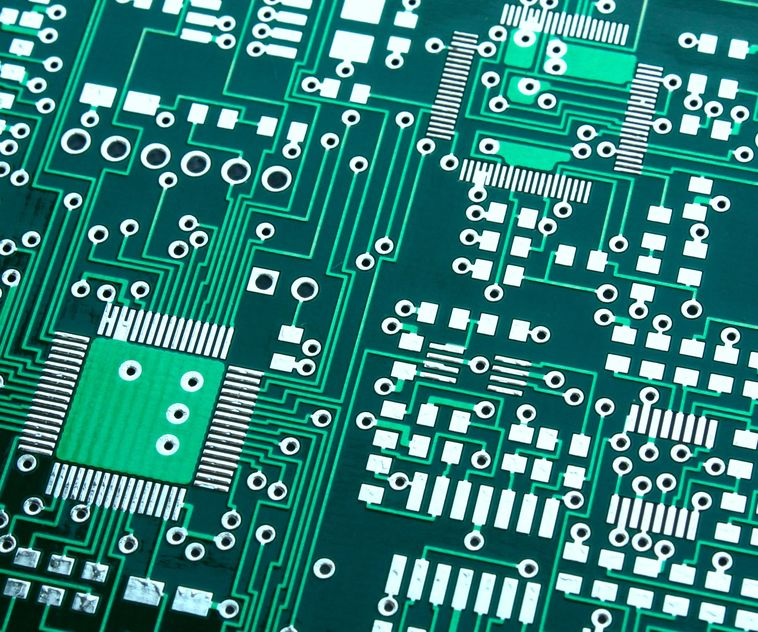
PRINTED CIRCUIT BAORDS or PCBs are circuit boards that have a printed distribution which direct and electrically or mechanically support your electrical components to be placed on your board, it has traces, wires and designed compartments for your components. The word PCB might not ring a bell in your ears but they could be found anywhere, if you open up a remote that controls your T.V you would see a little board which would be installed in the structure, that is your printed circuit board or your PCB.
PCBs play a vital role in modern day as technology is advancing and improving every single day.
Printed circuit boards serve as a base or a foundation for electronic products as these boards are being used in almost every electronic device.
They are variety of places where PCBs can be found few are mentioned in the text below:-
· Transformers
· Capacitors
· Electrical equipments like electromagnets
· Cable insulation
FABRICATION OF A PRINTED CIRCUIT BOARD (PCB):-
To fabricate a PCB means to perform a procedure which transform or transcribe a circuit board design to the real thing or transform the design in the physical structure following the instructions by a manufacturer.
PCB Fabrication comes after designing a PCB first, once a PCB has been designed fabrication follows after.
For fabrication there are some factors which are to be considered for example a good PCB prototype is required because a bad prototype would delay the making of PCBs.
A PCB should also be assembled the correct way to avoid time delay.
Avoiding manufacturing hang-ups would let you work where there is no factor that would delay the process of fabrication.
There are steps that should be taken to perfectly fabricate a PCB which are mentioned below:-
1. PCBS WITH PROPER SPECIFICATIONS:-Preparing your printed circuit board with proper traces, width and spacing so that later on there will be no mistakes when you will be sending your PCB for fabrication.
2. RIGHT POWER SUPPLY:-You should be aware of picking the right power supply which is able to provide optimum power supply to every component which is installed in your board.
3. CHOOSING RIGHT COMPONENETS BEFORE HAND:-In the designing phase which is just before fabrication phase already picking the right components to be placed during the fabrication process as the right components make your circuit board design perfect.
4. COMPONENETS LIKE CAPACITORS:-Components like capacitors or resistors should be picked before to prepare your PCB for fabrication.
5. BEST HEAT SUPPLY:-The perfect heat supply is also mandatory for PCB fabrication. Some PCBs are highly temperature resistive, if the temperature is too hot or too cold a PCB could have expansion or contraction which would cause abruption in traces or the wirings on the board.
6. FOLLOWING ALONG THE MANUFACTURER:-It’s best to follow the instructions that have been given to you by the manufacturer because if you follow the instructions there will be less possibilities for mistakes and a quick way to fabricate the PCB.
7. OPTIMIZING YOUR PCB DESIGN:-Optimizing your PCB design and ensuring the signal integrity to avoid Radio-frequency and electromagnetic waves to cause interference.
8. DOUBLE CHECKING THE DESIGN PROVIDED:-The rules which have been provided for deigning should be double checked because common mistakes like tracing could occur so double checking your board’s design would avoid such errors.
9. DOUBLE CHECKING THE CONNECTIONS:-Double checking the connections and the routes which have been designed.
10. DOUBLE CHECKING THE COMPONENTS ATTACHED:-Checking if the components are attached to the source signal or not.
11. UPDATING THE SIL SCREEN:-Updating the silk screen for data codes or PCB versioning etc.
GOING THROUGH EVERYTHING:-
It is important to understand how Printed circuit boards and their fabrication is important and significant in a journey of making a PCB. Fabrication of a PCB helps one out in PCB development, production and sometimes even into PCB operation.
PCB fabrication is an extremely important step which helps to manufacture your PCB along with assembly of your PCB.
Basically by making sure that you are following the guidelines and all the instructions that are provided by the manufacturer and by being completely sure that you have followed them correctly will end you with a safer fabrication process.
Following the rules of designing and double checking each step would help a student or electronic engineers and all the people working in this line of work for a safe and an error free fabrication procedure.
A fabrication process takes up to about 3 to 14 business days, the days are dependent upon specificities. Some parameters like how accurately a board has been designed and it will obviously would take more time if there is a time delay due to a mistake that has been caused in the phase of designing a board.
Typically printed circuit boards are prepared with in three to five days this number would exceed if there is an error and there would be a sudden emergency to redo a lot of your work so it is better to be very cautious and vigilant before the fabrication phase.

