
GPU PCB:Structure, Function and Design Complete Guide
KEY DEFINITION A GPU PCB is a multilayer printed circuit board designed to mount the graphics processing unit (GPU), memory modules, and power delivery circuitry while routing ultra-high-speed signals between them. Consumer graphics cards typically use 6 to 14 layers, while AI server-class boards supporting accelerators such as NVIDIA H100 or GB200 require 20 to 40+ layers, ultra-low-loss laminates, and any-layer HDI construction to support multi-terabit interconnects and power loads exceeding 700W.
Pull the heatsink off any graphics card and the chip underneath looks almost incidental compared to the board it sits on. That board is doing more engineering work than the GPU itself gets credit for.
This guide covers what a GPU PCB actually does, how it gets designed and built, where consumer and AI server boards diverge, and what separates a board built for a gaming card from one built for a rack full of accelerators.
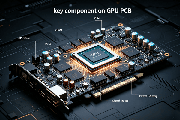
Key Components on a GPU PCB
A modern GPU board integrates several functional blocks, each responsible for stability, performance, or communication.
1. GPU Core (Graphics Processor)
The GPU die is the central compute engine. It executes parallel workloads such as rendering, AI inference, or matrix operations. It depends heavily on stable power delivery and high-speed memory access provided by the PCB.
2. VRAM (Video Memory)
GDDR6 or GDDR6X memory chips store textures, frame buffers, and compute data. These chips sit close to the GPU to minimize trace length and signal delay. Memory routing is one of the most impedance-sensitive parts of PCB design.
3. VRM (Voltage Regulator Module)
The VRM converts 12V input power into multiple low-voltage rails required by the GPU and memory. It consists of MOSFETs, inductors (chokes), and capacitors.
A well-designed VRM reduces voltage ripple and improves stability under sustained load. Poor VRM design typically results in throttling or system crashes during peak power draw.
4. Clock and Control ICs
These chips manage timing, voltage monitoring, and system control. They ensure synchronization between GPU core, memory, and PCIe interface.
5. PCIe Interface
The PCIe edge connector provides data communication between the GPU and the host CPU. High-speed lanes require strict impedance control and minimal signal loss.
6. Auxiliary Power Connectors
Modern GPUs use 8-pin, 12-pin, or 12VHPWR connectors to deliver additional power beyond PCIe slot limits. These inputs feed directly into the VRM network.
What a GPU PCB Actually Does
1. The Core Functions of a GPU PCB
A GPU PCB is not just a mounting surface, it performs four distinct functions that keep a graphics card running. Here is what each one actually does.
2. Fixed components
The board provides the physical surface where every critical part gets placed and electrically connected, including the GPU die, memory chips, voltage regulator circuitry, display connectors, and supporting control chips. Without a stable mounting surface, none of these parts could maintain the precise positioning that high-speed signal routing depends on.
3. Signal Transmission & Communication
Copper traces etched into the board carry data between the GPU and every other component on the card. These traces are what let the GPU pull instructions and exchange data with memory chips fast enough to keep up with gigahertz-level clock speeds.
4. Power Distribution & Delivery
Voltage regulator modules built into the board convert incoming power into the clean, stable voltage rails the GPU and memory chips require to operate without throttling. A poorly designed power delivery network shows up as instability or reduced performance under heavy load.
5. Structural Support
The board's material and construction give the card enough rigidity to survive installation, transport, and the physical stress of a mounted heatsink. FR4 fiberglass remains the standard substrate for this because it balances strength, cost, and electrical performance.
GPU PCB Design Considerations (Critical but Often Overlooked)
Designing a GPU PCB is not just routing components. It is a multi-variable optimization problem involving signal integrity, thermal behavior, and manufacturability.
1. Stack-Up Design
Layer count is determined by routing density and power requirements:
4–6 layers: Entry-level GPUs
8–14 layers: Mainstream to high-end GPUs
20–40+ layers: AI accelerator and server boards
Each additional layer supports either signal routing, ground return paths, or power distribution.
2. Impedance Control
High-speed signals (PCIe, GDDR, NVLink) require controlled impedance traces, typically 50Ω single-ended or 100Ω differential.
Even small variations in dielectric thickness or copper weight can affect signal timing at high frequencies.
3. Power Integrity Design
GPU power delivery is highly transient. Load can jump from idle to hundreds of amps in microseconds.
Key design practices include:
Multi-phase VRM distribution
Decoupling capacitor placement near GPU pads
Wide copper pours for low resistance current paths
4. Thermal-Aware Layout
Heat does not only come from the GPU die. VRMs and memory modules also generate significant thermal load.
Good PCB design:
Spreads VRMs across airflow paths
Avoids clustering high-loss components
Uses thermal vias under hot zones
5. Material Selection
Standard FR4 works for consumer boards, but high-speed AI systems require:
Low-loss or ultra-low-loss laminates
Stable dielectric constant (Dk) across temperature
Low dissipation factor (Df) for signal integrity
AI server PCBs often move away from FR4 entirely for this reason.
6. Manufacturability (DFM Reality Check)
A design that works in simulation may fail in production if:
Via aspect ratios are too aggressive
Layer registration tolerance is too tight
Copper balance is uneven across stack-up
Design-for-manufacturing is especially critical for 20+ layer HDI boards.
Why AI Server PCBs Are Fundamentally Different
AI server boards are not scaled-up gaming PCBs. They introduce entirely different constraints:
1. Signal Density
Multi-terabit interconnects require far more routing layers and tighter coupling control.
2. Power Scale
700W+ per accelerator requires extreme current handling and redundant power planes.
3. Material Cost
Ultra-low-loss laminates can cost several times more than standard FR4, often becoming a major portion of board cost.
4. Reliability Requirements
Server boards are expected to run continuously under full load, often in rack environments with limited airflow and high ambient temperature.
How GPU PCBs Differ Across Performance Tiers
GPU PCB design scales mainly across layer count, VRM complexity, and material requirements, with each tier reflecting increasing demands for power stability and high-speed signal integrity.
| Tier | Example | PCB Layer Count | Power Design | Key Characteristics |
|---|---|---|---|---|
| Entry-Level GPU | AMD RX 6400 | ~4 layers | 3+1 phases | Cost-driven design, minimal VRM cooling, limited overclocking headroom |
| Mainstream GPU | NVIDIA RTX 3060 Ti | ~8 layers | ~7+1 phases | Balanced performance and cost, improved thermal and power stability |
| Enthusiast GPU | ASUS RTX 3090 Strix | ~10 layers | ~18–20 phases | High-current VRM design, premium components, reinforced thermal/backplate structure |
| AI Compute Board | NVIDIA H100 | ~22 layers | Server-grade multi-phase VRM | High-density routing, strict impedance control, sustained 700W+ workloads |
| AI Scale-Out / Switch Board | GB300 / NVSwitch (GB200 NVL72) | ~22–40 layers | Distributed high-power architecture | Any-layer HDI, ultra-low-loss materials, multi-terabit interconnect support |
That jump from consumer boards to AI server boards is not incremental. It is a different manufacturing problem, which is why sourcing strategy needs to match the tier.
Why Work With PCBgogo for GPU and AI Server PCB Projects
Sourcing a GPU board, especially one built for AI accelerator workloads, means working with a manufacturer who can actually hold registration across 20 plus layers, handle ultra-low-loss laminates without delamination, and run BGA assembly clean enough for a 700W chip to run reliably for years. Getting any one of those wrong turns into a board respin, and a board respin on an AI accelerator project is an expensive way to lose a quarter.
At PCBgogo, we manufacture high-layer-count multilayer and HDI boards built for exactly this kind of demanding GPU and AI server work, with the process control needed to hold tight impedance tolerances and clean BGA assembly across high component density designs. Our production and inspection workflow is built around consistent board quality and dependable turnaround, so you are not choosing between speed and a board that actually performs under sustained load. If you are sourcing a GPU PCB or AI server PCB project, reach out and tell us what you are building, and our team will get back to you with a tailored manufacturing plan and quote.
Final Takeaway
A GPU PCB is not just a mounting surface, it is the signal, power, and thermal backbone that determines whether a chip can actually hit its rated performance. As GPUs scale from consumer cards into AI accelerator territory, layer counts, materials, and manufacturing precision scale right along with them, so matching your manufacturing partner to your tier matters as much as the design itself.
Frequently Asked Questions
What is the difference between a GPU PCB and an AI server PCB?
A consumer GPU PCB typically runs 4 to 14 layers on standard or mid-loss laminate, built for a single graphics card. An AI server PCB supporting accelerators like the H100 or GB200 runs 20 to 40 plus layers on ultra-low-loss material, built to handle multi-terabit interconnects and far higher power loads across a rack of GPUs.
Why do AI server PCBs need so many more layers than gaming GPU boards?
AI accelerator boards route extremely high-speed interconnects like NVLink between multiple GPUs and switches, and each additional signal plane, power plane, and ground plane needed to maintain signal integrity at those data rates adds another layer to the stack-up.
What is a VRM and why does it matter on a GPU PCB?
A VRM, or voltage regulator module, converts incoming power into the stable voltage rails a GPU needs to run without instability. Weak or insufficient VRM design causes voltage ripple that can throttle performance or cause crashes under sustained load.
Why do AI server PCBs cost so much more per square meter than standard boards?
The jump comes from material grade, not just layer count. Ultra-low-loss laminates used in AI server boards can cost six to twenty times more than standard FR4, and each additional layer adds its own lamination, drilling, and plating cost on top of that.
Does a higher layer count always mean better GPU performance?
Not directly. Layer count supports the signal routing, power delivery, and EMI control a high-performance GPU needs, but performance ultimately depends on the chip itself, with the PCB acting as the foundation that lets the chip reach its rated speed reliably.


