
DIP Assembly Process: 5 Key Steps and 3 Challenges
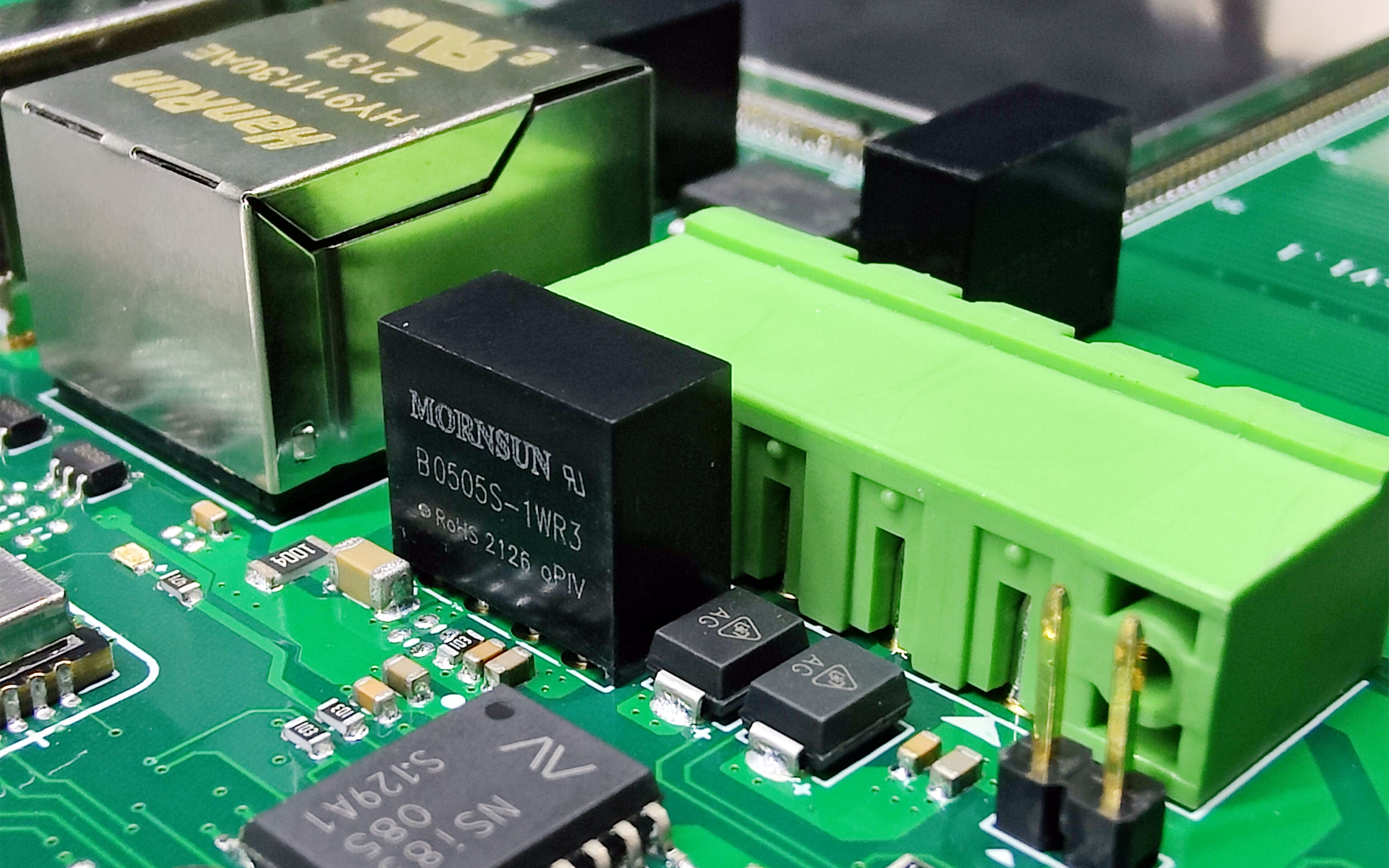
While Surface Mount Technology (SMT) dominates modern electronics manufacturing, the DIP Assembly Process (Dual In-line Package), which utilizes through-hole technology, remains a vital and essential part of PCBA Manufacturing. This process is necessary for components that are too large, handle high power, or have irregular shapes, making them unsuitable for automated SMT placement. These include large connectors, relays, power resistors, and transformers. The DIP Assembly Process ensures these components are robustly and permanently affixed to the Printed Circuit Board (PCB).
Understanding the systematic flow and critical control points of the DIP Assembly Process is fundamental to ensuring the long-term reliability of any electronic product that utilizes both through-hole and surface-mount components.
The Five-Stage DIP Assembly Process Flow
The DIP Assembly Process is typically executed after the SMT components have already been placed and reflowed onto the board. This order minimizes thermal stress on the larger through-hole parts.
1. Component Insertion (Plugging)
This is the initial placement stage where the leads of the through-hole components (THCs) are inserted into the corresponding plated holes on the PCB.
Procedure: This can be performed manually by skilled operators, or automatically using dedicated Automatic Insertion Machines for high-volume jobs with standardized components (like axial or radial parts).
Quality Check: Strict verification is required to ensure components are correctly oriented (polarity) and securely seated against the board surface, without any misalignment or damage.
2. Adhesion (Dispensing/Curing)
For certain large or heavy components, particularly those that may experience vibration or mechanical stress, an industrial adhesive (often an epoxy) is applied before the subsequent soldering phase.
Function: This step provides added mechanical stability, preventing the components from lifting or shifting during the high-stress environment of Wave Soldering.
3. Wave Soldering
This is the main automated soldering step for through-hole components. The PCBA is passed over a wave of molten solder. * Process Stages:
* Flux Application: A liquid flux is sprayed onto the bottom of the board to clean the metal surfaces and promote solder wetting.
* Preheating: The board is heated to activate the flux and prevent thermal shock when the board hits the molten solder.
* Solder Wave Contact: The board passes over a wave of molten solder, which flows up through the component holes to form the metallic joints.
* Cooling: The board cools, solidifying the solder joints.
4. Lead Trimming (Cutting)
After the soldering is complete, the excess component leads that protrude from the underside of the board are cut to a uniform and appropriate length.
Purpose: This critical post-soldering step prevents potential short circuits with the product enclosure or other circuitry and prepares the PCBA for subsequent assembly stages.
5. Inspection and Functional Testing
The final and most crucial step for quality assurance.
Visual Inspection (QC): Checking for common defects such as solder bridges, insufficient solder, missing components, or incorrect polarity.
Functional Testing: The completed PCBA is subjected to electrical tests (often In-Circuit Testing (ICT) or functional tests) to verify that the electronic device operates according to design specifications.
Essential Quality Control Considerations
To ensure the reliability and longevity of products utilizing the DIP Assembly Process, specific precautions must be maintained throughout the workflow:
ESD Control: Due to the manual handling inherent in the DIP Assembly Process, strict Electrostatic Discharge (ESD) protective measures—including grounding straps, conductive mats, and proper handling procedures—are non-negotiable to protect sensitive components.
Component Insertion Integrity: Operators must adhere rigidly to the Bill of Materials (BOM) and assembly drawings to prevent misplacement, incorrect orientation, or damage to component leads.
Wave Soldering Profile Management: The Wave Soldering equipment requires routine maintenance. Crucially, the temperature profile (preheat, flux activity, and wave contact time) must be precisely controlled to ensure effective soldering without damaging heat-sensitive components.
Conclusion: Relying on Experts for the DIP Assembly Process
The DIP Assembly Process, though often manual or semi-automated, is a fundamental pillar of modern PCBA Manufacturing. The quality of the final product hinges on meticulously controlling component insertion, Wave Soldering parameters, and rigorous inspection protocols. For complex products requiring both high-precision SMT and reliable through-hole integration, choosing a manufacturing partner with deep expertise in the entire spectrum of assembly processes is vital.
PCBGOGO provides end-to-end PCBA Manufacturing Services, mastering both advanced SMT and reliable DIP Assembly Processes to deliver superior quality and reliability. We ensure every through-hole component is mounted and soldered to the highest industrial standards. Contact PCBGOGO today to discuss your complete PCBA needs, from component sourcing to final assembly and testing.

