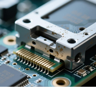
Corrosion Protection in PCB Shielding Connection Design:3 Critical Details
The interface where a shield meets the circuit board is the most vulnerable point in any electronic assembly. At PCBGOGO, our analysis of field failures shows that over 80% of shielding-related issues originate at this specific junction. If the PCB shielding connection design fails to account for environmental factors, corrosion at the contact points will degrade EMI blocking and may produce conductive oxidation layers that lead to catastrophic short circuits. To ensure long-term reliability, engineers must implement these three critical anti-corrosion details.

1. Optimize Joining Methods to Eliminate Crevice Corrosion
Crevice corrosion is the most common threat at the shield-to-board interface. When small gaps exist between the shield and the PCB, moisture and corrosive gases become trapped, creating a stagnant micro-environment that accelerates metal decay.
Soldering: This is the preferred method for high-reliability applications. Soldering creates a continuous, hermetic seal that eliminates gaps. While traditional wave soldering can sometimes cause mechanical stress or deformation, PCBGOGO recommends laser or precision manual soldering to ensure a high-quality, gap-free bond.
Snap-on Clips: These are convenient for maintenance and assembly but inherently leave gaps. If your design requires a snap-on shield, we recommend adding a sealing gasket (such as silicone or conductive rubber) at the contact points to block moisture ingress.
For industrial or outdoor electronics, a soldered PCB shielding connection design provides the most robust defense against crevice-driven decay.
2. Standardize Surface Finishes to Prevent Galvanic Corrosion
Galvanic corrosion occurs when two dissimilar metals are in electrical contact within an electrolyte (like humidity or salt spray). For example, a galvanized steel shield attached to a tin-plated PCB pad creates a "battery" effect where the zinc acts as an anode and corrodes rapidly.
The key to a successful PCB shielding connection design is ensuring electrochemical compatibility:
Material Matching: Always aim for identical surface treatments. If the shield is nickel-plated, the PCB pads should also utilize a nickel-based finish (like ENIG).
Insulating Barriers: In extreme cases, a conformal coating (liquid wrap) can be applied to the joint to isolate the metal from the environment. However, ensure the coating does not break the ground path required for EMI suppression.
3. Implement Drainage and Ventilation to Prevent Moisture Traps
Standing water is the ultimate catalyst for corrosion. In humid environments, condensation often collects at the base of the shield, leading to rapid oxidation of the solder joints.
Micro-Drainage Holes: Engineers should include small drainage ports (typically 0.5mm to 1.0mm in diameter) at the lowest points of the shield. These ports allow moisture to escape without compromising the Faraday cage’s shielding effectiveness.
Ventilation Slots: Adding small slots in the PCB layout near the connection points promotes airflow and speeds up the evaporation of trapped condensation.
At PCBGOGO, we assist our clients in identifying the best positions for these features during the DFM (Design for Manufacturability) stage, significantly improving the lifespan of the PCB shielding connection design.
Conclusion
A shield is only as effective as its weakest point. By focusing on gap elimination, material compatibility, and moisture management, you can transform a standard PCB shielding connection design into a high-performance, corrosion-resistant system.
Partner with PCBGOGO for your next project. We provide expert fabrication and professional advice on how to protect your electronics from the harshest environments.

