
Best PCB Design Software: Top Picks for 2026 (Free & Paid)
Picking PCB design software feels a bit like choosing a car. A beginner does not need the same tool as an engineer routing a sixteen layer server board, and the wrong choice early on can mean re-learning an entire workflow later.
This guide breaks down the strongest free and paid PCB design software available right now, what each one does best, and how to know when it is time to upgrade.
What to Look for in PCB Design Software
Good PCB design software comes down to a few core factors:
Layer and routing capability: free tools are often capped at two to four layers; paid tools typically support unlimited layers for complex boards
Simulation accuracy: real time SPICE simulation catches circuit issues before fabrication, reducing costly respins
Design rule checking (DRC): automated clearance and connectivity checks save hours on larger boards
Library and component management: how easily you can find, reuse, and organize footprints across projects
Team workflow fit: version control and multi user editing matter once more than one engineer touches a design
The core question to ask: are you designing a one off project, or a product you plan to manufacture and revise repeatedly? That answer usually determines whether free or paid software makes sense.
1. KiCad: The Best Free PCB Design Software Overall
KiCad is a free, open source PCB design tool with no restrictions on layer count, board size, or commercial use. Key strengths include:
No licensing fees at any stage, from prototyping to volume manufacturing
Built in SPICE simulation through ngspice, no separate software needed
3D board viewer for checking component fit before ordering
Thousands of free community footprints and symbols, maintained by an active open source community
KiCad is the natural starting point for makers, students, and small teams who want professional grade tools without a subscription.
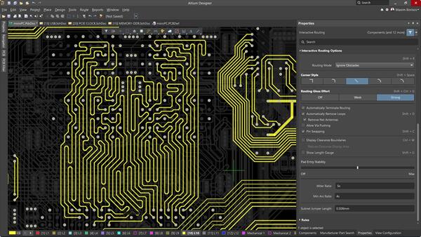
2. Altium Designer: Best for Professional Engineering Teams
Altium Designer is a paid, subscription based tool built for engineers managing complex, high layer count boards under tight deadlines. It stands out for:
Real time design rule checking that flags routing and clearance issues as you work, not after the fact
Strong library management and version control, useful once multiple engineers edit the same design
Integration with mechanical CAD tools, streamlining handoff between electrical and mechanical teams
Teams that need guaranteed support and frequent updates generally find Altium's cost justified by the time saved on large projects.
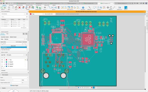
3. Fusion 360 Electronics: Best for Mechanical and Electrical Co-Design
Fusion 360 Electronics, built on the former Eagle platform, is Autodesk's PCB tool for teams that need electrical and mechanical design in one environment. It lets engineers see how a PCB fits inside its enclosure in real time, cutting down the back and forth between electrical and mechanical teams. This makes it a strong fit for consumer electronics and product design work, where board shape and enclosure fit matter as much as routing itself.
4. Cadence Allegro and OrCAD: Best for Enterprise Scale Designs
Cadence's Allegro and OrCAD platforms are built for enterprise level PCB design, common in aerospace, telecom, and server hardware:
OrCAD handles schematic capture and simulation
Allegro focuses on advanced layout and manufacturing preparation
Both platforms support boards with dozens of layers and strict signal integrity requirements
The learning curve is steep and the cost is significant, but for large engineering organizations, the depth of control is often necessary.
5. DesignSpark PCB: A Free Alternative Backed by a Component Distributor
DesignSpark PCB is a free tool from RS Components that pairs schematic capture and PCB layout with direct access to RS's component library and pricing data. Unlike KiCad's community driven model, DesignSpark is maintained by a commercial distributor, offering steadier long term support but a smaller independent user community. It suits engineers who want a no cost tool with built in access to real, purchasable component data during the design phase.
6. Flux.ai: An AI-Assisted Option Worth Watching
Flux.ai is a browser based PCB design tool that adds an AI copilot to schematic capture and layout, suggesting components and catching common design errors as you work. It reflects a broader shift toward AI assisted workflows that reduce repetitive tasks like footprint selection and initial routing. It is not yet a replacement for established tools on complex boards, but it is worth watching as AI continues to reshape PCB design.
Free vs Paid: When to Upgrade
The table below compares core capabilities across free and paid tiers to help clarify when an upgrade actually pays off.
| Software | Cost | Layer Limit | Best For |
|---|---|---|---|
| KiCad | Free | Unlimited | Hobbyists, startups, students |
| DesignSpark PCB | Free | Limited by version | Component sourcing focused design |
| Altium Designer | Paid (subscription) | Unlimited | Professional teams, complex boards |
| Cadence Allegro / OrCAD | Paid (enterprise) | Unlimited, high speed | Aerospace, telecom, server hardware |
According to IPC-2221, the generic standard for PCB design, layer count and spacing requirements scale significantly with signal speed and current load, which is exactly where paid tools' advanced design rule checking earns its cost. If you are designing a board for personal use or a low volume product, KiCad covers nearly everything you need. Once you are managing multiple engineers or boards with strict signal integrity requirements, the time saved by a paid tool's automation typically outweighs the subscription cost.
From Design File to Manufactured Board
Once your layout is finalized, getting it built correctly comes down to a few concrete steps:
Export your Gerber files (or ODB++) along with your BOM and pick and place files if assembly is needed
Double check your design rules against your chosen manufacturer's capabilities, especially minimum trace width and hole size
Submit for a manufacturability review before committing to production, catching issues early is far cheaper than reworking after fabrication
PCBgogo works directly with Gerber and BOM files exported from any of the tools above, and its team reviews designs for manufacturability before production starts, helping catch issues before they turn into costly reworks.
FAQs
What is the best free PCB design software for beginners?
KiCad is the best starting point because it has no layer or board size limits and a large library of free community made footprints. It has a steeper initial learning curve than some tools, but the skills transfer directly to professional work later.
Is KiCad good enough for professional use?
Yes, KiCad is used commercially by companies of all sizes, including for products that ship at volume. It lacks some enterprise features like built in version control, but many teams pair it with external tools like Git to manage that gap.
Can I use free PCB design software for commercial products?
Most free PCB design tools, including KiCad and DesignSpark PCB, allow commercial use without licensing fees. Always check the specific license terms of any tool before shipping a commercial product, since terms can change between versions.
How do I go from PCB design software to a manufactured board?
Export your Gerber files, BOM, and pick and place files, then send them to a manufacturer for a design for manufacturability review. PCBgogo, for example, checks files for issues before production starts, so problems get caught before they become expensive reworks.
Conclusion
There is no single best PCB design software, only the best fit for your project's scale and budget. KiCad covers most individual and small team needs at zero cost, while Altium and Cadence's tools take over once complexity and team size grow. Whichever tool you choose, PCBgogo can turn your finished design into a manufactured board with a quick file review before production.


