
Advanced PCB - Needs, Design, and Manufacturing
The construction of 5G facilitate the growth of the PCB industry. As the "mother of electronic products", PCB applies to most of electronic products such as communications, mobile phones, computers, and automobiles. The total demand for terminals and base stations increases leading to growth of the electronic application. the demand for PCBs will increase.
At present, major manufacturers have developed advanced Micro-LED PCB and high-frequency advanced PCB manufacturing technology to respond to the development of 5G, IoT and AI. They accelerate the packaging and substrate of related products as well as components.

Image courtesy: Samsung
Throughout the overall industry development trend, the global PCB industry is making progress in high density, high precision, and high capability. By reducing costs, improving PCB performance, and reducing environmental impact, PCB fabrication adapt to downstream electronic terminal equipment, where HDI (High Density Interconnect), FPC (Flexible Printed Circuit), rigid-flex board and IC substrate will become the focus of future development.
The HF (high-frequency) PCB is made from FR4 glass fiber board by using a whole piece of epoxy glass cloth. It is a branch of advanced PCB. The color of the whole HF PCB is relatively bright. Its density is greater than the standard PCB. Generally, HF PCBs are used in circuits with frequencies above 1G. The characteristic is dielectric constant, which must be stable with low dielectric loss, leading to good performance against water-absorption and moisture without compensation on heat resistance, corrosion resistance.
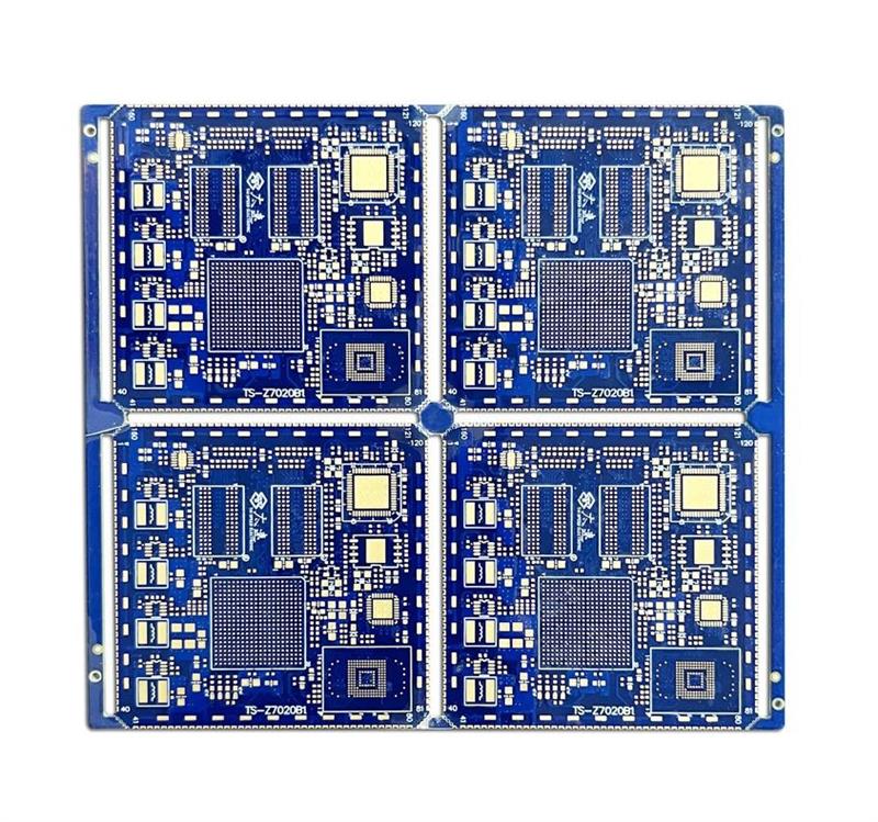
Image courtesy: PCBgogo HDI PCB
Advanced PCB is a high power density inverter (High Density Inverter), a printed circuit board with relatively high line distribution density using micro blind buried via technology. It is a compact product designed for small capacity users. It adopts modular parallel design, one module capacity is 1000VA (1U), natural cooling, can be directly put into a 19" rack, and can be connected in parallel with a maximum of 6 modules. The product adopts full digital signal process control (DSP) technology and multiple A patented technology, with full-range adaptive load capacity and strong short-time overload capacity.
The Original Name of Advanced PCB
Many other names have been used in the industry to describe HDI PCB, which is a kind of advanced PCB. For example, western have termed them SBU (Sequence Build Up Process) because of the sequential building process in production, while the manufacturing process used by Japanese manufacturers is called MVP (Micro Via Process) because of the small pore structure. Besides, it is also called as BUM (Build Up Multilayer Board) in the past.
The IPC Connecting Electronics Industries in the United States suggests that this sort of product technology can be called as HDI (High Density Interconnection, High Density Interconnection) technology to prevent misunderstanding.
Advanced PCB Prototype - Blind & Buried Via PCB, 10 Layers HDI PCB
With the current portable product trending, PCB design is moving toward downsizing and high density, increasing the demands on the high-tech PCB manufacturing process. Blind and buried vias are used in BGA packages,≤0.65mm pitch. Mostly used in portable productions.
1. What are the differences between blind vias and buried vias?
Most of them are small holes with a diameter from 0.05mm to 0.15mm. The drilling methods of buried blind holes include laser drilling, plasma etching and photoforming.
(Blind vias / Laser Vias): Blind vias are the type of vias that connect the PCB inner layer traces to the PCB surface traces, which do not penetrate the entire board.
(Buried vias): Buried vias are the type of vias that only connect the traces between the inner layers, so they cannot be seen from the surface of the PCB.
The figure is a schematic diagram of the cross-sectional structure of an 8-layer board:
A: Through hole (L1-L8)
B: Buried vias (L2-L7)
C: Blind hole (L7-L8)
D: Blind hole (L1-L3)

Note: The examples use 8-layer board as an example
The following figure is the cross-sectional structure of the blind buried via seen in the Navigator window of the PADS Router (BlazeRouter):
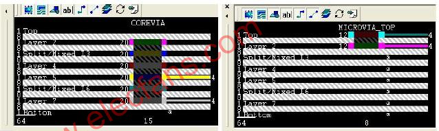
Buried vias of Layer2-Layer7 Layer1-Blind vias of Layer2
Printed circuit boards, also known as PCB, are often used in the application of high-end products such as mobile phones and GPS. The structure of a conventional multi-layer circuit board consists of inner and outer layers, drilling holes, and etc. The integrated process is used to realize the connection function between the inner parts of each layer of the circuit.
2. The precautions And Maintenance of Advanced PCB Prototype
2.1 Precautions
If you want to copy the PCB, the difficulty is relatively high. Generally, blind and buried holes will be encountered when copying the PCB on the mobile phone, pay attention to the following matters:
1. Be careful and make preparations before copying the PCB;
2. The equipment must be advanced;
3. In the process of copying, it is necessary to constantly compare it with the original PCB;
4. Pay attention to the inspection and remind of double check.
2.2 Maintenance
In order to ensure the good working condition of the blind and buried via PCB and reduce the failure rate of such kind of PCBs in production, it is necessary to maintain the PCB, including annual maintenance and semi-maintenance. The maintenance methods are as follows.
2.2.1 Annual maintenance of blind and buried holes
(1) Regularly check the capacity of the electrolytic capacitor in the PCB. When the capacity of the electrolytic capacitor is found to be lower than 20% of the nominal capacity, it should be replaced in time; in general, the shelf life of the electrolytic capacitor is about 10 years. As a result, all electrolytic capacitors should be replaced in about 10 years.
(2) For high-power devices coated with heat-dissipating silicone grease, check whether the heat-dissipating silicone grease is dry or solid. The high-power devices in the PCB are burned out due to poor heat dissipation.
(3) Clean up the dust on the PCB in time.
2.2.2 Semi-maintenance of blind and buried holes
(1) Clean the dust on the PCB every week by using the special cleaning solution for it. After cleaning the dust on the PCB, dry the PCB in time.
(2) Observe whether the electronic components in the PCB have undergone high temperature traces, and whether the electrolytic capacitor bulge or leak, and if so, it should be replaced.
Electronic products moves towards high density and high precision, the same requirements are put forward for blind & buried vias PCB as well as HDI PCB. PCBgogo is an experienced advanced PCB manufacturing company who offered quick-turn PCB prototype and PCB assembly services. A trustworthy PCB company that have satisfied hundreds of engineers’ demand for years.


