
Advanced Diagnosis and Handling of BGA Soldering Defects in SMT Assembly
Ball Grid Array (BGA) components are essential to modern electronics, offering high I/O density and superior electrical performance. However, due to their intricate design—where solder joints are concealed beneath the package—they pose unique challenges during Surface Mount Technology (SMT assembly). The presence of BGA Soldering Defects can severely compromise the reliability and functionality of a Printed Circuit Board Assembly (PCBA), necessitating rigorous process control and advanced diagnostic techniques. Understanding the typical failure modes and their root causes is paramount for high-yield manufacturing.
Common Failure Modes in BGA Assembly
Effective troubleshooting begins with identifying the specific type of defect. Key BGA Soldering Defects include:
Solder Bridging (Short Circuits): The unintended connection of adjacent solder balls, leading to electrical shorts.
Solder Voiding (Empty Cavities): Air or flux entrapped within the solidified solder joint, which reduces the joint's mechanical strength and electrical conductivity. This can significantly impact the component's thermal path.
Non-Wet/Cold Solder Joints: Characterized by a dull, grainy appearance, indicating incomplete reflow or insufficient thermal energy, resulting in a weak, unreliable connection.
Solder Skewing (Elongation): Uneven height or shape of solder balls, often resulting from excessive paste volume or inconsistent pressure during placement.
Pad Misalignment: Positional deviation between the BGA's solder sphere and the corresponding PCB land pad, caused by inaccurate component placement.
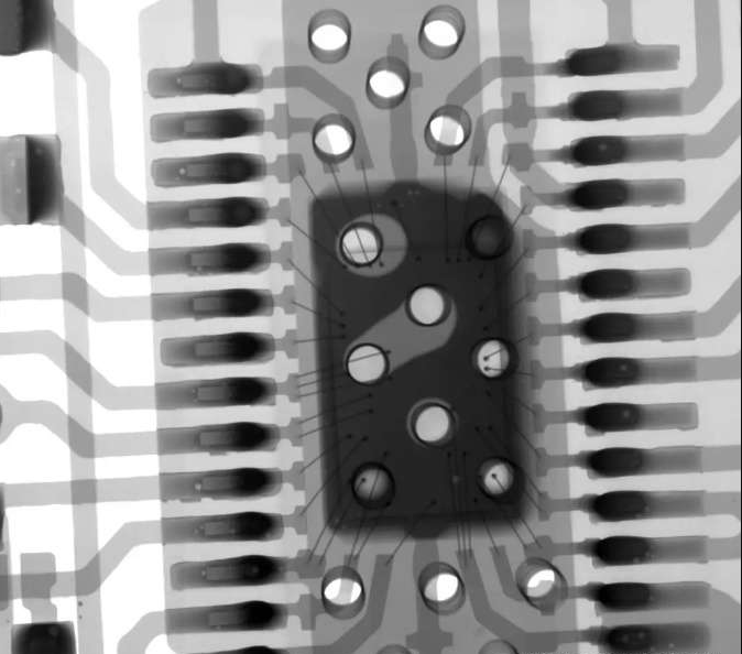
Advanced Diagnostic and Inspection Methods
Unlike standard components, BGA defects cannot be visually inspected post-reflow. Therefore, specialized techniques are mandatory:
Non-Destructive Testing (NDT):
X-ray Inspection: This is the industry-standard method. A high-resolution X-ray inspection system utilizes X-ray penetration to visualize the hidden solder joints. It accurately detects internal faults like solder voiding, bridging, opens (non-wetting), and component tilt/floating. This method is crucial for ensuring compliance with IPC standards.
Destructive Testing:
Micro-Sectioning (Cross-Sectioning): Involves carefully cutting and polishing the PCBA through the BGA solder joints for microscopic analysis. This technique provides detailed structural insight into the intermetallic compound formation, internal integrity, and overall solder volume.
Root Causes and Process Optimization
Addressing BGA Soldering Defects requires systematic control over the manufacturing process:
Conclusion: Achieving Zero-Defect BGA Soldering with Expert SMT Assembly
Mitigating BGA Soldering Defects is not a reactive fix but a proactive commitment to quality management throughout the SMT assembly line. It demands precision placement, rigorous thermal control, and advanced non-destructive inspection capabilities.
For businesses seeking unparalleled reliability in their electronic products, partnering with an expert full-service manufacturer is essential. PCBGOGO is a trusted global provider, renowned for its expertise in high-precision PCBA manufacturing. We utilize advanced BGA placement systems, meticulously calibrated reflow ovens, and state-of-the-art X-ray inspection equipment to ensure robust BGA joints and minimize defects. By choosing PCBGOGO, you leverage our decades of experience in complex SMT assembly and component-level quality control, guaranteeing exceptional reliability for your critical applications.

