
AI Glasses PCB Miniaturization Design Guide
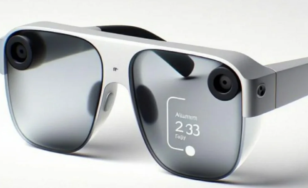
As AI glasses continue to pursue ultra-lightweight wearability, the internal PCB must fit into extremely limited spaces—typically within 20 mm × 30 mm—while still integrating a processor, sensors, power management, and wireless modules (Wi-Fi 6 / Bluetooth 5.3).
Industry data shows that 60% of AI glasses R&D failures are caused by insufficient PCB miniaturization. One manufacturer even delayed launch by three months because their PCB exceeded 25×35 mm, resulting in only 65% assembly yield at the glasses frame.
With 5 years of micro-PCB expertise, PCBGOGO has delivered 800,000+ small-form-factor PCBs, reaching minimum sizes down to 12×15 mm, serving over 30 leading AR/VR brands.
This guide breaks down the core design parameters, engineering constraints, and integration strategies that help hardware engineers overcome miniaturization bottlenecks.
1. Key Technologies in AI Glasses PCB Miniaturization
Miniaturizing PCB designs for AI glasses must follow IPC-2221 Section 5.4 guidelines on micro-PCB design. The challenge focuses on three engineering limits:
1) Fine Line Widths & Micro-Vias
Traditional PCB: 0.2 mm line width, 0.3 mm hole size
AI glasses PCB: 0.12–0.15 mm line width, 0.15–0.20 mm via diameter
Must meet GB/T 4677 tolerance ±0.05 mm
PCBGOGO's lab tests show:
Line width <0.12 mm increases etching break-risk by 30%
Requires semi-additive process (SAP) for stability
2) High-Density Layer Stack
Standard consumer PCB: 4–6 layers
AI glasses: 8–12 layers, often with 3+2+3 symmetric HDI stacking
Interlayer thickness: 0.08–0.10 mm
IPC-A-600G Class 3 bubble rate requirement: ≤1%
3) Ultra-Small Component Integration
Use of 01005 components (0.4×0.2 mm)
Placement accuracy must reach ±0.02 mm
Otherwise component shift rate can exceed 15%, especially around high-density SoCs and RF areas
Recommended Base Materials
| Material | Thickness | Tg / Dk | Best Use |
|---|---|---|---|
| Shengyi S2116 | 0.1–0.3 mm | Tg=165°C | Mainstream AI glasses |
| Rogers RO4350B | 0.15–0.4 mm | Dk=4.4±0.05 | High-frequency / AR navigation modules |
Both materials pass PCBGOGO micro-PCB qualification and support stable 0.12 mm line-width mass production.
3. Practical Miniaturization Solutions
3.1 Four-Step Miniaturization Method
Step 1 — Layer Stack Planning
A typical 8-layer AI glasses PCB can use:
Signal – GND – Power – Signal – Signal – Power – GND – Signal
Laminates: Shengyi S2116 at 0.15 mm / layer
Prepreg: Panasonic R-1515, 0.05 mm per sheet
Thickness tolerance: ±0.01 mm
Stackup generated via PCBGOGO JPE-Layer 5.0
Step 2 — Defining Line Widths & Via Sizes
Signal lines: 0.15 mm (1 oz copper), 50 Ω impedance
Computed using Z = 60/√εr × ln(5.98h/W) with h=0.1 mm
Power lines: 0.20 mm (supports 1 A current)
Micro-vias: 0.20 mm, drilling accuracy ±0.01 mm
Fabricated using PCBGOGO JPE-Laser-600
Step 3 — Component Layout Strategy
Follow: functional zoning + shortest routing
Processor (Qualcomm XR2 Gen 2) centered for heat symmetry
Cameras & microphones arranged around edges
Wi-Fi 6 module placed outward to reduce interference
Component spacing: ≥0.1 mm
Altium Designer 23 + PCBGOGO DFM (JPE-DFM 7.0) for collision detection
Step 4 — Routing Optimization
High-frequency lines (Wi-Fi 6) routed on surface layer; impedance controlled at 47.5–52.5 Ω
Avoid vias for power traces to minimize IR drop
Add ground shielding ≥0.1 mm for sensor signals following IPC-2221 6.2
3.2 Manufacturing Reliability Measures
Semi-Additive Etching Process (SAP)
Thin copper deposition: 5 μm → patterning → plating up to 35 μm (1 oz)
Achieves ±0.01 mm line-width precision
Follows IPC-TM-650 2.3.17
Solder Mask Coating
Liquid photo-imageable type (JPE-SR-800)
Thickness 15–20 μm
Coverage >0.05 mm to prevent creeping onto pads
Dimensional Inspection
Per-batch sampling: 50 pcs
Measured via JPE-Vision-900 at ±0.001 mm accuracy
Dimensional yield target: ≥99.5%
Conclusion
Miniaturizing AI glasses PCBs requires a balanced combination of:
High-density layer stacking
Micro-scale line width & via reduction
01005 component integration
Advanced processes like semi-additive manufacturing
Through its micro-PCB ecosystem—DFM pre-review, 0.1 mm laser drilling, SAP fine-line etching, and full-dimension inspection—PCBGOGO enables hardware engineers to confidently turn ultra-small PCB designs into reliable mass-production reality.

