
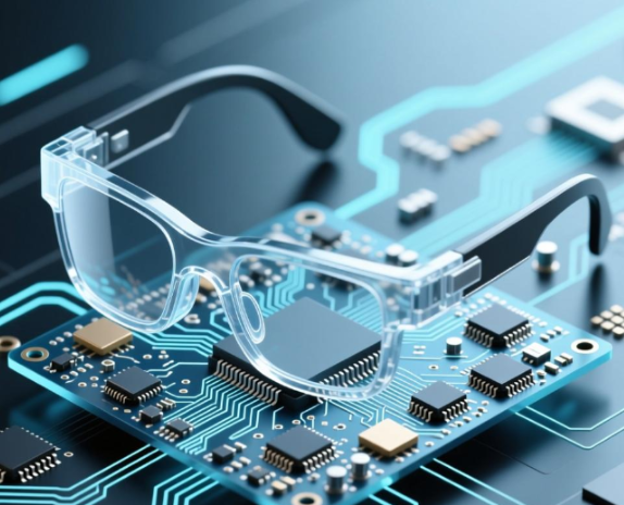
AI Glasses PCB Low-Power Design: A Practical Guide for Power Engineers
AI smart glasses rely on compact lithium batteries (typically 300–500 mAh), yet the PCB alone can consume 20–30% of the total system power. Industry reports show that unoptimized AI-glasses PCBs often reach static current over 50 mA and dynamic current beyond 300 mA, resulting in only 3–4 hours of battery life—far below users’ expectations of 6+ hours.
One AR glasses manufacturer once faced a 40% drop in sales after launch due to severe “poor battery life” complaints caused by excessive PCB power loss.
With more than six years of experience in low-power PCB design, PCBGOGO has developed AI-glasses PCB solutions achieving:
Static current ≤ 30 mA
Dynamic current ≤ 220 mA
Battery life extended to 5.5 hours and beyond
This article breaks down the root causes of PCB power loss, explains layout and thermal optimization methods, and provides actionable solutions tailored for power engineers.
1. Core Technical Analysis
PCB power consumption in AI glasses mainly comes from:
(A) Power Trace Losses
According to IPC-2221 Section 5.2 and GB/T 19226 Section 4.3, power-line loss is determined by copper resistance:
R=ρLSR = \rho \frac{L}{S}R=ρSL
Where
ρ = copper resistivity
L = trace length
S = cross-sectional area
Typical PCB with 0.2 mm trace width + 1 oz copper has ~0.5 Ω/m resistance. At 1 A load, this means 0.5 W loss.
Optimized design with 0.3 mm trace width + 2 oz copper reduces resistance to 0.2 Ω/m, lowering loss to 0.2 W—a 60% reduction.
(B) Thermal Inefficiency
Poor heat dissipation increases chip power use:
Every +10°C → ~8% higher chip power
A processor rising from 40°C to 60°C = 16% more power consumption
This follows IPC-9701 Section 3.2, emphasizing thermal management for high-density boards.
Key Requirements for Low-Power AI Glasses PCB
Power trace copper ≥ 2 oz (70 μm)
Local power delivery (distance from power module to chip ≤ 10 mm)
Thermal relief windows under processors per IPC-2221 Section 7.3
2. Practical Low-Power Design Solutions
2.1 Four-Step Low-Power Engineering Method
1. Power Trace Optimization
Main power line (3.7 V battery → PMU):
Width: 0.3–0.4 mm, Copper: 2 oz, Resistance ≤ 0.2 Ω/m
Branch supply for sensors:
Width 0.2 mm, Copper 1.5 oz, Resistance ≤ 0.3 Ω/m
Trace length: avoid detours, keep ≤ 15 mm; processor power trace ≤ 10 mm
2. Grounding Optimization
Use single-point grounding (signal GND + power GND tied at PCB edge)
→ Avoids ground loops that can add 10–15% additional powerGround trace copper ≥ 2 oz, width ≥ 0.3 mm, resistance ≤ 50 mΩ
(IPC-2221 Section 6.1)
3. Thermal Design
Under processor/Wi-Fi modules:
Use copper pour with thermal windows
Area ≥ 1.5× chip footprint, no solder mask for better heat spreading
Chip-to-chip spacing ≥ 0.5 mm to avoid local heat stacking
Use higher thermal conductivity laminates:
Example: Shengyi S1130, 0.35 W/m·K, ~25% higher than standard FR-4
4. Component Selection
Use low-power SoCs (e.g., Qualcomm XR2 Gen 2 low-power variant, static ≤ 10 mA)
Add an LDO at PMU output:
Example: TI TPS7A4700, static current only 1 μA
Reduces voltage ripple and prevents unnecessary power spikes
3.2 Power Verification & Optimization Workflow
1. Static Power Testing
Using a precision DC analyzer (e.g., JPE-DCA-600, ±1 μA):
Target static current: ≤ 30 mA
2. Dynamic Load Testing
Processor + Wi-Fi + sensors fully active:
Current ≤ 220 mA
Total power ≤ 0.814 W (3.7 V × 0.22 A)
3. Thermal Testing
After 1 hour full load, using IR thermal camera (JPE-IR-800):
Chip temperature ≤ 55°C
Above 60°C requires redesign per IPC-9701 Section 4.1
Conclusion
Low-power PCB design for AI glasses revolves around two engineering goals:
1. Reduce electrical losses
(Thicker copper, shorter traces, optimized grounding)
2. Improve thermal efficiency
(Copper windows, better materials, spacing)
With enhanced layout, low-power chips, and LDO stabilization, PCB efficiency can directly extend AI glasses battery life. PCBGOGO offers complete low-power design + simulation + power testing services, ensuring your AI glasses PCB meets strict power and thermal requirements before mass production.

