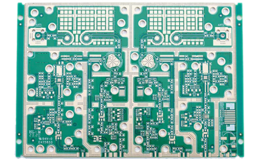
4 Key Design Strategies to Prevent PCB Through-Hole Pad Solder Spill
In the complete chain of PCB fabrication and assembly, the design stage serves as the first line of defense for product quality. To fundamentally prevent solder spill on through-hole pads, engineers must integrate spill-prevention principles during the PCB design phase instead of relying on corrective actions during assembly. Drawing from PCBGOGO’s experience in integrated PCB design and manufacturing, the following techniques highlight how to control solder spill at its source.

1. Optimal Pad and Drill Size Ratio: Core Principle for Spill Prevention
A common misconception in PCB design is assuming that the closer the fit between the hole diameter and component lead, the stronger the solder joint. However, when the gap is less than 0.1 mm, molten solder cannot flow and fill efficiently, causing pressure buildup and overflow onto the pad surface. Conversely, if the gap exceeds 0.3 mm, excessive solder volume increases the spill.
According to PCBGOGO’s design criteria:
The drill diameter should exceed the pin diameter by 0.15–0.25 mm
The pad diameter should exceed the drill diameter by 0.6–0.8 mm
This ratio allows sufficient solder fill while utilizing surface tension to keep solder within the pad boundary and reduce spill risk.
2. Accurate Solder Mask Opening Control
Solder mask is not only for insulation and board protection; it also functions as a physical barrier for solder containment. The opening diameter directly influences solder distribution.
Oversized openings remove containment capability and allow solder to spread beyond the pad
Undersized openings reduce pad exposure, increasing edge overflow
PCBGOGO recommends:
Solder mask opening 0.1–0.2 mm smaller than the pad diameter
Clearance between the opening edge and drill edge ≥ 0.2 mm
This approach preserves functional pad area while forming a containment boundary that mitigates solder spill during wave or reflow soldering.
3. Applying Non-Standard Pad Shapes for Special Scenarios
For HDI layouts or high-current through-hole connections, standard round pads may not sufficiently control solder behavior. In these scenarios, non-standard geometries improve stability.
Applicable designs include:
Teardrop pads: Smooth transition between trace and pad increases adhesion strength, preventing spill at the trace junction
Square pads: Larger surface area boosts surface tension, particularly useful for large-diameter holes
PCBGOGO has deployed teardrop pad designs extensively in EV (electric vehicle) power PCBs, effectively reducing spill issues in high-current environments.
4. Stack-Up Planning and Through-Hole Type Selection
For multilayer PCBs, selecting the appropriate via type can structurally eliminate solder spill at the board surface.
Blind vias connect outer layers to adjacent layers only
Buried vias remain fully internal and require minimal solder fill
Compared with full through-holes, these vias do not transmit solder to the opposite side, inherently removing reverse-side spill risk. Additionally, when planning inner copper layers, engineers should avoid placing large copper pours directly beneath through-holes. Excessive heat conduction accelerates solder solidification, leading to inadequate fill and localized spill.
Conclusion: Design Determines Reliability
Design defines PCB performance and determines the probability of solder spill long before production begins. By applying the correct pad-to-hole ratios, calibrated solder mask openings, shaped pad structures, and appropriate via selection, spill-related defects can be minimized from the source.
With a dedicated engineering team and complete process verification system, PCBGOGO provides end-to-end services from design optimization to volume production, enabling customers to achieve higher soldering reliability and product consistency.

