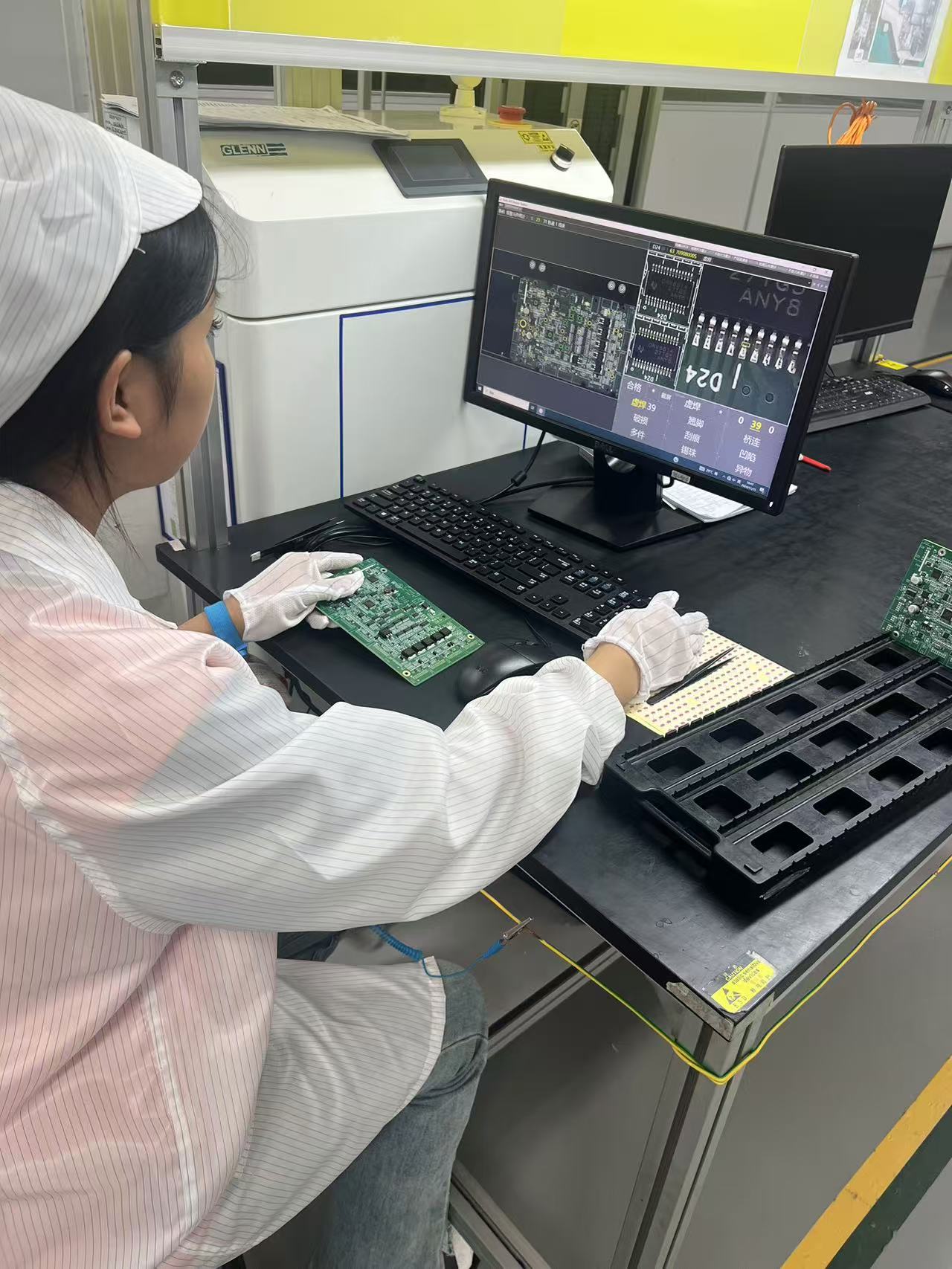
3D AOI vs 2D AOI: Which Inspection Technology Delivers Better SMT Quality?
In the world of Surface Mount Technology (SMT), achieving flawless Printed Circuit Board (PCB) assembly requires rigorous quality control. The primary tool for this is Automated Optical Inspection (AOI). While 2D AOI was the industry standard for years, the advanced capabilities of 3D AOI have made it the superior choice for modern, high-density, high-reliability PCBs.
The core difference lies in their ability to measure the crucial Z-axis (height). This seemingly simple addition allows 3D AOI to capture defects that are literally invisible to its 2D counterpart, leading to a massive leap in SMT quality.

3D AOI vs 2D AOI: Understanding the Technologies
2D AOI: The Flat Image
2D AOI systems use a single, high-resolution camera positioned directly over the PCB.
How it Works: It captures a flat, two-dimensional image of the board's surface. Inspection relies heavily on contrast and pattern recognition (comparing the image to a "golden" reference board or CAD data).
Strengths: Excellent for detecting planar defects:
Missing components
Component Misalignment (X/Y axis)
Incorrect polarity (if marked clearly)
Severe solder bridges (shorts)
Limitation: It cannot measure height or volume. Defects that rely on a height differential, such as insufficient solder, lifted leads, or component tilt, are often missed or result in high false calls (false alarms) due to shadows and reflections.
3D AOI: The Topographical Map
3D AOI systems build upon 2D technology by incorporating structured light projection (often a pattern of light or laser triangulation) and multiple cameras.
How it Works: The structured light pattern is projected onto the PCB. The height and contours of the components and solder joints distort this pattern. Multiple cameras then capture this distortion, allowing the system's software to calculate the exact height, volume, and shape of every feature, creating a true three-dimensional map of the board.
Strengths: Provides metrology-grade accuracy by measuring the Z-axis, leading to superior defect detection and process control.
The Three-Dimensional Advantage: Key Differences
Why 3D AOI Delivers Better SMT Quality?
The ability to measure the Z-axis provides two critical quality improvements:
1. Real Solder Joint Assessment (Volumetric Measurement)
A poor solder joint might look perfectly fine in a flat 2D image, but a 3D system can confirm that the volume of solder is insufficient to form a reliable connection. This is crucial for modern miniaturized components, where the tolerances for solder paste volume are extremely tight. 3D AOI identifies defects like:
Insufficient Solder: The most common Z-axis defect.
Head-in-Pillow (HIP): A complex BGA defect where the solder ball and paste touch but fail to coalesce.
Solder Fillet Shape: Ensuring the solder forms a strong, reliable connection geometry.
2. Process Control and Yield Optimization
Because 3D AOI provides quantitative, measurable height data, it can be used for true Statistical Process Control (SPC). Manufacturers don't just know if a board passed, they know the average solder height and component tilt across the entire batch. This data provides invaluable feedback to upstream machines (like the stencil printer and pick-and-place machine), allowing engineers to proactively adjust the process, minimizing defects before they even occur and dramatically increasing the first-pass yield.
When Is 2D AOI Still Useful?
Despite its limitations, 2D AOI is still valuable for:
Cost-controlled SMT production
Boards with low-to-medium density
Simple components (0402, 0603, SOT, SMD capacitors/resistors)
Early-stage prototyping
Many factories use both technologies—2D AOI for general detection and 3D AOI for precision-critical areas.
Conclusion: Investing in Quality with 3D Inspection
While 2D AOI remains a viable, cost-effective option for simpler PCB designs, the evolution of electronics—with smaller components and tighter pitch—has made 3D AOI the necessary standard for superior SMT quality. Its ability to accurately measure volume, height, and coplanarity translates directly into fewer false positives, reduced rework, and ultimately, a more reliable end product.
For designers and engineers demanding the highest level of quality assurance, partnering with a manufacturer who utilizes this advanced technology is essential. That's why at PCBGOGO, we prioritize integrating advanced inspection methods like 3D AOI into our SMT assembly process. By leveraging these cutting-edge tools, we ensure your complex, high-density PCBs meet the stringent reliability standards required for today's market.

