
Unveiling the Future: How Novel Materials Are Reshaping PCB Manufacturing
The printed circuit board (PCB), the foundational backbone of nearly all modern electronics, has long been defined by its conventional materials and processes. For decades, the duo of copper and fiberglass (FR-4) has been the industry standard, processed through well-established techniques like chemical etching and electroplating. Yet, as the demand for smaller, faster, and more powerful devices accelerates, these traditional methods are hitting their physical limits. The industry is at a critical inflection point, and the future of PCB manufacturing isn't just about tweaking old processes—it's about a fundamental shift driven by revolutionary new materials.
Today, a new generation of materials, including carbon nanotubes, graphene, and various advanced polymers, are poised to redefine what's possible in PCB design and production. They promise not just incremental improvements but a radical leap forward in performance and functionality.
Carbon Nanotubes (CNTs): The Next-Generation Thermal and Electrical Conduit
Carbon nanotubes, cylindrical structures of carbon atoms, are lauded for their extraordinary properties. When incorporated into PCBs, they can significantly enhance both thermal and electrical performance.
Superior Thermal Management: One of the most pressing challenges in high-density PCBs is heat dissipation. As components become more compact and powerful, the risk of overheating and performance degradation increases. CNTs, with a thermal conductivity far surpassing that of copper, can be used to create highly efficient thermal vias and heat sinks directly within the board's substrate. This allows for a more even distribution of heat, protecting sensitive components and enabling higher operational speeds.
Enhanced Electron Migration Resistance: In ultra-fine traces, copper can suffer from electron migration, a process where electrons push metal atoms out of place, leading to shorts or open circuits over time. CNTs possess an incredible current-carrying capacity and are highly resistant to this phenomenon, making them an ideal candidate for creating durable, ultra-thin traces in high-frequency circuits.
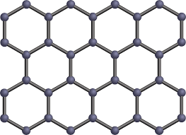
Graphene: The Unparalleled Conductor for a New Era of Electronics
Graphene, a single layer of carbon atoms arranged in a honeycomb lattice, is another game-changer. Its unique properties make it a compelling alternative to traditional copper.
Exceptional Electrical Conductivity: Graphene is known as one of the most conductive materials on Earth. Its integration into PCB traces can dramatically reduce signal loss and improve signal integrity, which is crucial for high-speed digital and RF applications. This allows for the design of smaller, more efficient boards that can handle higher data rates without signal degradation.
Superior Mechanical Strength: Beyond its electrical properties, graphene is also incredibly strong and flexible. This opens up new possibilities for flexible and stretchable electronics, a rapidly growing market segment. Imagine smart textiles, wearable sensors, and medical devices where the PCB can bend and conform to a user's body without breaking. Graphene-based traces can provide the necessary mechanical resilience for these applications.
Redefining Traditional Manufacturing Processes
The introduction of these novel materials is not a simple drop-in replacement. It requires a fundamental rethinking of traditional PCB manufacturing processes.
Beyond Etching and Plating: Traditional subtractive processes, which involve etching away unwanted copper, are wasteful and often ill-suited for the micro-scale features required by today’s technology. Instead, additive manufacturing techniques, like printing conductive inks containing graphene or CNTs, are gaining traction. These methods are more precise, consume less material, and enable the creation of complex, multi-layered structures with greater ease.
Challenges of Cost and Scalability: While the potential is immense, integrating these materials into large-scale production presents significant challenges. The cost of raw materials and the specialized equipment needed for deposition and processing remain high. The industry is actively researching and developing new, cost-effective methods for mass production, but this hurdle must be cleared for widespread adoption. The transition will be a phased one, likely starting with high-end, specialized applications before moving into mainstream consumer electronics.
Conclusion: Our Perspective on the Road Ahead
As a leading player in the PCB fabrication industry, we at PCBgogo have our fingers on the pulse of these revolutionary developments. We're not just observing; we are actively exploring and investing in the research and development of these advanced manufacturing techniques. We believe the future of electronics lies in pushing beyond the limitations of current materials and processes. We are committed to pioneering new solutions, from refining our high-frequency board capabilities to exploring the integration of new materials that can solve our customers' most complex design challenges.
The era of conventional PCB manufacturing is gradually giving way to a new age of innovation. The adoption of materials like carbon nanotubes and graphene isn't just a trend; it's the inevitable evolution needed to power the next generation of smart, connected, and high-performance devices. And we, here at PCBgogo, are excited to be at the forefront of this transformation, ready to help our partners build the future.

