
The Green Transition Path of the PCB Industry Under Heavy Environmental Pressure
With the development of the electronics industry, printed circuit boards (PCBs), as the core components of electronic products, have an increasingly prominent contradiction between their production and environmental protection. Against the backdrop of growing global environmental awareness, the PCB industry is facing severe environmental challenges, and green transformation has become an inevitable choice for its sustainable development.
Stringent Environmental Regulations: A Burden on the PCB Industry
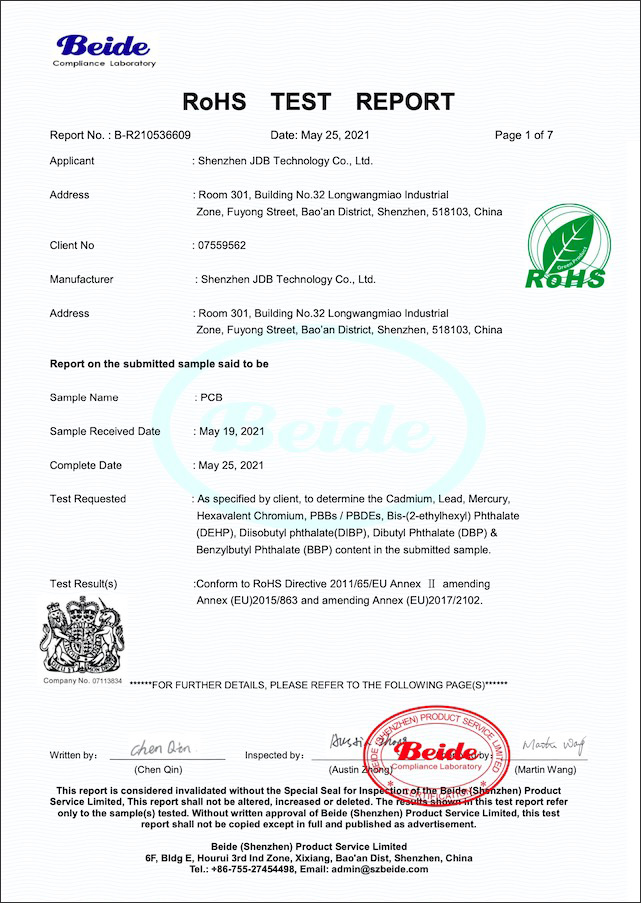
Global environmental regulations are becoming increasingly strict. The European Union's Restriction of Hazardous Substances (RoHS) directive restricts the use of harmful substances such as lead and mercury, while China's "Evaluation Guidelines for Green Factories in the Electronic Information Manufacturing Industry" regulates enterprises' resource utilization and sewage discharge behaviors.
These regulations have forced PCB enterprises to invest huge amounts of money in environmental protection transformation. The transformation costs for medium-sized enterprises range from millions to tens of millions of yuan, which significantly increases the operating costs of enterprises and brings pressure to the entire industry.
Current Situation of the PCB Industry: Severe Pollution from Traditional Processes
Traditional production processes have caused a lot of pollution. In terms of raw materials, brominated flame retardants, solvent-based inks (with a volatile organic compound content of 30%), and lead-containing solders pose risks of releasing toxic gases, causing pollution, and lead hazards.
In the production process, the etching and electroplating processes will produce wastewater containing heavy metals, polluting water bodies and soil; high-temperature processes consume a lot of energy, exacerbating carbon emissions; if solid wastes such as glass fiber dust and waste circuit boards are not handled properly, they will also cause harm to the environment.
Exploration of Green Transition Paths
Material Innovation: Green Source
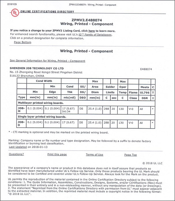
1.Halogen-free flame-retardant substrates: Phosphorus-based, nitrogen-based and other substrates can reduce combustion smoke by 70%, reduce toxicity, meet the UL94 V0 standard, comply with RoHS 2.0 requirements, and have UL certification, improving environmental performance.
2.Water-based inks and lead-free solders: Water-based inks can reduce volatile organic compound emissions by 90%; lead-free solders eliminate lead pollution and also increase the recycling value of solder dross.
3.Degradable auxiliary materials: The application of paper-based tapes, plant-based solvents, etc., reduces the environmental burden of the entire production process.
Process Upgrade: Clean Production
1.Water circulation system: Through closed-loop treatment, the reuse rate of water exceeds 90%, and some enterprises have achieved zero discharge of sewage.
2.Energy optimization: Heat pump heating reduces energy consumption by 40%, solar panels meet 20% of electricity demand, and artificial intelligence load regulation reduces unit energy consumption from 8 kWh/square meter to 5 kWh/square meter.
3.Clean technologies: Laser Direct Imaging (LDI) technology reduces chemical processes, dry etching reduces chemical usage by 70%, and electroplating lines can recover 95% of metal ions.
Circular Economy: Turning Waste into Treasure
1.Waste recycling: Etching copper slag with a copper content of 30% can be refined to obtain pure copper for reuse; glass fiber dust is made into insulating materials.
2.Recycling and utilization of old PCBs: Waste PCBs can be used to extract copper, gold (about 200 grams per ton), etc., and non-metallic parts are made into recycled substrates, forming a closed-loop system.
3.By-product value-added: Nickel slag generated from electroplating is made into battery materials, and iron ions in etching solution are converted into water treatment agents, becoming new sources of income.
Transformation Challenges and Countermeasures
Challenges
1.Technical difficulties: The performance of degradable materials is insufficient, and the lamination process of multi-layer boards needs to be optimized.
2.High costs: Huge investments in research and development, equipment, etc., are unbearable for small and medium-sized enterprises, and the operation and maintenance costs are relatively high.
3.Low market awareness: Consumers and downstream enterprises prefer low-cost traditional products, which increases the difficulty of promotion.
Countermeasures
1.Technical cooperation: Enterprises cooperate with scientific research institutions to develop new materials and improve their performance.
2.Cost control and obtaining support: Strive for government preferential subsidies, and enterprises themselves reduce costs by optimizing processes.
3.Strengthen promotion: Publicize the advantages of green products through activities such as exhibitions to guide market demand.
Conclusion: PCBgogo's Position
PCBgogo firmly believes in the importance of green transformation, actively adopts environmentally friendly materials, optimizes production processes to reduce consumption, and explores recycling models.
We are well aware that transformation is both a responsibility and an opportunity. We will continue to move forward, leading the PCB industry to achieve sustainable development and contributing to global environmental protection.

