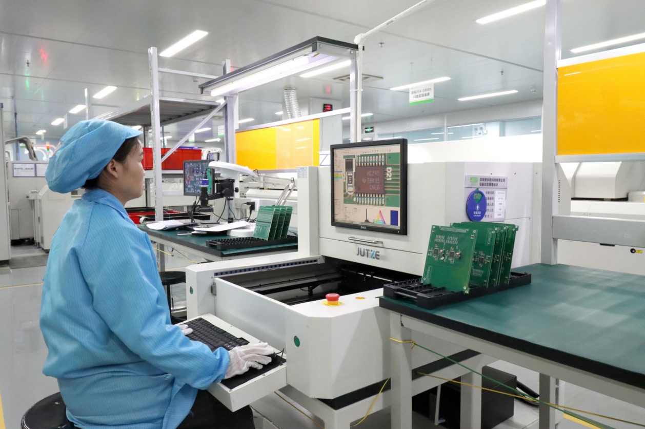
RF PCB Design for Manufacturability: Key Strategies
Introduction: Unique Demands of RF PCB Design
Radio Frequency (RF) circuits are essential in communication, radar, and wireless technologies. Due to their high signal frequencies, RF printed circuit boards (PCBs) demand greater precision than conventional digital or analog designs. Designers must balance electrical performance with signal integrity, electromagnetic compatibility, and thermal management. One of the most pressing concerns is ensuring manufacturability without compromising performance.

Challenges in RF PCB Manufacturing
1. Signal Loss and Transmission Efficiency
High-frequency signals are more vulnerable to loss, distortion, and reflection during transmission. Issues like conductor resistance, inductive and capacitive effects in traces, and improper layout can degrade signal quality. Minimizing loss and ensuring consistent transmission paths are primary design concerns.
2. Impedance Control and Matching
Effective impedance matching is vital to prevent reflection and crosstalk. Poor design can destabilize entire systems. Precise trace width calculation and dielectric thickness control are essential to maintaining consistent impedance—typically targeting 50Ω or 75Ω.
3. Electromagnetic Interference (EMI)
RF signals are particularly susceptible to EMI due to their radiative properties. Poor grounding, irregular trace routing, or power integrity issues can amplify interference. Careful layout and shielding are necessary to preserve signal fidelity.
4. Heat Management
Power-intensive RF circuits generate considerable heat, potentially leading to component failure or signal degradation. Managing thermal load through board structure and material choice is a key aspect of durable turnkey manufacturing for RF systems.
Engineering Principles for High-Performance RF PCBs
1. Minimizing Signal Loss
Loss arises from resistive, capacitive, and inductive parasitics. To mitigate it:
Material Selection: Opt for low-loss materials such as PTFE that exhibit low dielectric loss.
Trace Design: Keep traces short and direct to avoid unnecessary bends and maintain signal strength.
Shielding: Introduce shielding layers to reduce external interference and isolate signal pathways.
2. Ensuring Impedance Consistency
Mismatched impedance not only degrades signals but can compromise system stability:
Precise Trace Calculations: Base trace width on dielectric constant, signal frequency, and target impedance.
Dielectric Control: Maintain consistent dielectric layer thickness between PCB layers.
Use of Microstrip or Stripline: These transmission line structures offer excellent impedance control.
3. Combating EMI
Reducing EMI is crucial for reliable RF performance:
Ground Layer Optimization: Employ solid ground planes to create low-impedance return paths.
Decoupling Capacitors: Install decoupling caps between power and ground to suppress noise.
EMI Shields: Use metal shielding cans or copper pour to contain and protect RF signals.
4. Thermal Design Considerations
Effective thermal management extends board lifespan and enhances performance:
Thicker Copper Layers: Aid in rapid heat dissipation.
Thermal Vias: Connect hot components to bottom layers or heatsinks for efficient cooling.
High Thermal Conductivity Materials: Disperse heat evenly across the PCB.
Optimizing RF PCB Layout for Manufacturability
1. Layer Stackup Configuration
RF PCBs often require multilayer construction. Typical stacks pair inner signal layers with ground planes, while outer layers manage routing and shielding. This design improves isolation and enhances reliability.
2. Signal Path Planning
Direct and consistent routing is key. Avoid sharp corners and excessive via use. Straight, wide traces with minimal direction changes are essential in high-speed signal paths.
3. Material Suitability
Use materials like ceramics, PTFE, or high-frequency glass fiber composites. Their electrical properties must align with frequency and application requirements to minimize signal attenuation.
4. Thermal Enhancement for High-Power Designs
High-power RF boards need robust thermal solutions. Techniques like denser thermal vias, copper pours, and added heatsinks help maintain performance stability over time.
Conclusion
RF PCB design demands a careful balance of electrical, mechanical, and thermal factors to achieve reliable performance in complex environments. At PCBGOGO, we offer professional turnkey manufacturing services that streamline every stage—from design to printed circuit board testing—ensuring your RF projects meet both technical and production demands. Whether you're sourcing from a trusted pcb supplier or scaling up for production, thoughtful RF PCB design is the key to performance and reliability.

