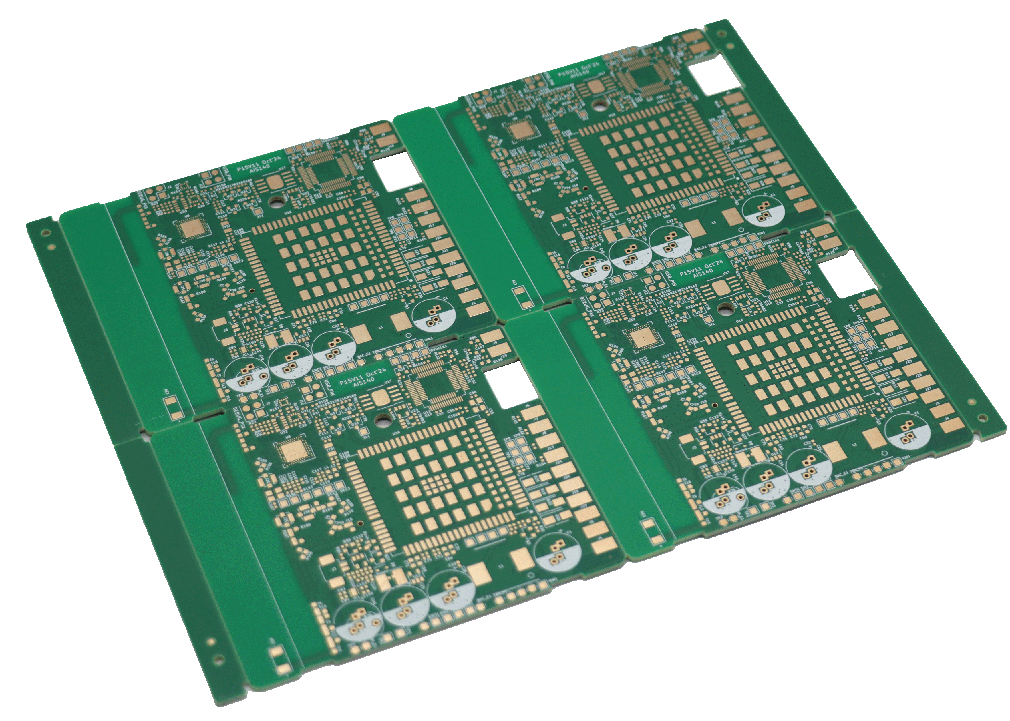
Photoresist Role in PCB Making
Have you ever wondered how intricate circuit patterns are precisely transferred onto a blank PCB? The unsung hero behind this process is the photoresist. Think of it as a high-precision "sunscreen" for copper. Wherever it covers, the copper remains protected during etching.
This light-sensitive layer is what enables the creation of complex, high-density circuits that power today's electronics. Without it, manufacturing modern PCBs would be nearly impossible. Let's break down how this crucial material works.
How Photoresist Works: A Three-Step Process
Application and Exposure: A uniform layer of liquid or dry film photoresist is applied to the clean copper surface. A photographic film containing the circuit design is placed on top. When exposed to ultraviolet (UV) light, the photoresist undergoes a chemical change. For a negative-tone resist (the most common type), the areas hit by UV light harden and become insoluble.
Development: Revealing the Pattern: The board is then "developed," much like a photograph. A chemical solution washes away the unhardened photoresist that was shielded from the UV light by the dark areas of the film. What remains is an exact negative image of the circuit pattern, with hardened resist protecting the copper traces that will form the final circuit.
Etching: The Final Transfer: The board enters the etching chamber, where a chemical spray (e.g., ferric chloride) dissolves away all the unprotected copper. The copper shielded by the hardened photoresist remains intact. Finally, the hardened resist itself is stripped away, revealing the pristine, finished copper circuit pattern.

Industry Trends and The Future of Photoresist
As electronics shrink and become more powerful, PCB traces and spaces are getting finer—down to 20 microns or less. This pushes photoresist technology to its limits. The industry is seeing several key trends:
Higher Resolution: New formulations of photoresist are essential for creating the ultra-fine lines required for High-Density Interconnect (HDI) PCBs and advanced packaging.
LDI Compatibility: Direct imaging systems that use lasers to expose the resist without a physical film are becoming standard. This requires photoresists optimized for specific laser wavelengths, offering greater accuracy and overcoming the limitations of traditional film-based exposure.
Advanced Processes: For the most demanding applications, processes like mSAP (modified Semi-Additive Process) rely on a thin photoresist layer to define the pattern for electroplating, showcasing a more sophisticated use of the material beyond simple etching.
Our Commitment at PCBgogo
At PCBgogo, we understand that the quality of the photoresist and the precision of its processing directly determine the accuracy and reliability of your boards. In an era where designs are increasingly complex, we invest in advanced exposure and developing equipment to ensure every micron of your circuit is perfectly defined. We carefully select our photoresist materials to meet the challenges of modern PCB manufacturing, from simple prototypes to complex HDI boards. Partner with us, and you'll get more than just a board; you'll get a product built with meticulous attention to the fundamental steps that guarantee performance.

