
PCB's "Surgical Procedure": How Backdrilling Solves the 5G Signal Reflection Problem
The journey of a high-speed signal on a PCB is a delicate one. As data rates climb into the multi-gigahertz range, even the tiniest imperfections can wreak havoc on signal integrity. In the era of 5G, where every bit of data counts, engineers face a particularly thorny issue: signal reflections caused by unused portions of through-hole vias. This problem, often subtle but destructive, can be the difference between a high-performing product and a failed one.
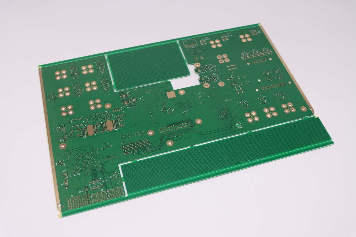
This is where a specialized manufacturing technique known as backdrilling comes in. Aptly named, it’s a process akin to a "surgical procedure" on a PCB, precisely removing the unnecessary parts of a via to ensure a clean signal path.
The Anatomy of a Problem: Via Stubs and Signal Reflections
To understand the need for backdrilling, you must first understand the culprit: the via stub.
A standard through-hole via, used to connect layers of a PCB, is a continuous, copper-plated hole that runs all the way from the top to the bottom of the board. When a high-frequency signal travels from one layer to another, it uses this via. However, if the signal doesn't use the entire length of the via—for instance, if it enters on Layer 2 and exits on Layer 4 of a 10-layer board—the remaining portion of the via (the part that extends from Layer 4 to the bottom layer) acts like a small antenna.
This unused portion, the "via stub," is a parasitic element. When the high-frequency signal reaches the end of the active via and encounters this stub, a portion of the signal "bounces back" or reflects. This reflection can cause significant signal degradation, including:
Signal loss: A weakened signal due to the reflected energy.
Signal distortion: The reflected signal interferes with the original, causing waveform distortion and an increase in bit error rate (BER).
Crosstalk: The via stub can radiate energy, interfering with adjacent signals.
For the multi-gigahertz signals used in 5G and high-speed data transmission, these effects are catastrophic. A clean signal is critical for maintaining high data throughput and system reliability.
The Surgical Solution: Backdrilling in Action
Backdrilling, also known as controlled depth drilling, is the precise removal of a via stub. The process works like this:
Standard Drilling: First, all through-hole vias are drilled as usual.
Backdrilling Setup: The board is then placed on the drilling machine again, this time with a special tool and a controlled depth program.
Precise Removal: The machine drills into the via from the opposite side of the signal's entry point, stopping just before it reaches the last layer used by the signal. This removes the "stub" without damaging the active signal path.
The result is a via that only exists on the layers it's needed for, effectively eliminating the parasitic antenna effect. The key to this process is the incredible precision required. The drill must be perfectly aligned and stop at the correct depth, leaving a small, clean gap between the end of the backdrill and the last layer connected to the signal.
The Role of Backdrilling in Today's Technology
Backdrilling has become a standard practice for a wide range of high-performance applications:
5G and Telecommunications: With data rates reaching 10 Gbps and beyond, backdrilling is a non-negotiable step for 5G base stations, routers, and other telecom equipment to ensure signal integrity.
High-Performance Computing: Server motherboards, supercomputers, and data center equipment rely on backdrilling to ensure clean data transmission between processors, memory, and high-speed interfaces.
Aerospace and Defense: In applications where reliability is paramount, backdrilling is used to ensure signal clarity in complex avionics and radar systems.
The trend is clear: as speeds increase, the need for backdrilling will only grow. It is no longer a niche, high-cost option but a necessity for any design pushing the boundaries of signal integrity.
At PCBgogo, Our Commitment to Precision
At PCBgogo, we understand that high-speed designs are built on precision. We have invested heavily in the advanced drilling technology and the expertise required to perform backdrilling with meticulous accuracy. We recognize that for your most demanding projects, from high-frequency RF boards to complex server motherboards, every detail matters.
Our goal is to be more than just a manufacturer; we aim to be a partner in your engineering journey. By offering advanced capabilities like backdrilling, we empower you to design with confidence, knowing that the final product will perform exactly as you intended, free from the hidden signal integrity issues that can derail even the best designs. We are proud to be at the forefront of this technology, providing the "surgical" precision your next-generation projects demand.

